
This post is going to be yet another part of the previous camera projects published on this blog. As described in the last post here in which i made Raspberry PI camera Sony IMX219 4 Lane MIPI CSI Board.
In this post will be having details about how to get data out of MIPI camera, make it useable and then feed data into Cypress FX3 USB3.0 controller.


 |
| Full Frame 8Mpixel Capture |
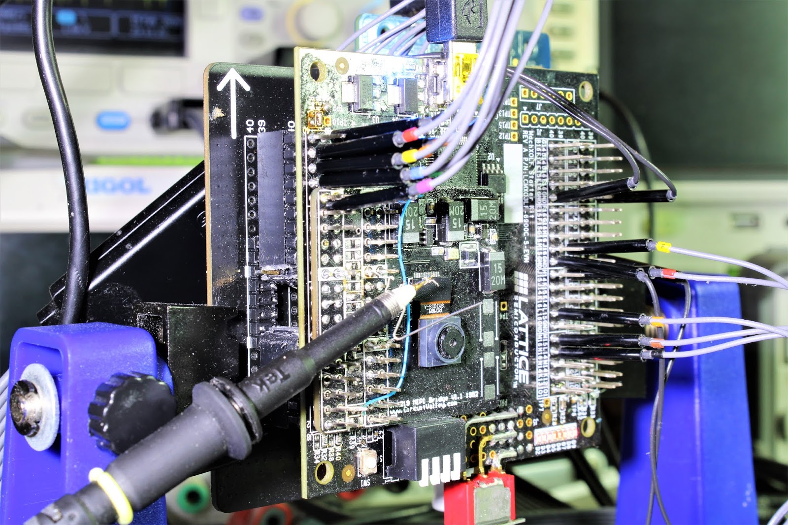
Lattice MachXO3 FPGA Cypress FX3 Interrconnect Inter Connect PCB
Camera module Directy connects to the FPGA Board and FPGA board Connects to Cypress FX3 FPGA board using this interconnect. There is not much in this PCB only few regulators for VCCIO
and length match 32bit 100Mhz bus for FPGA to FX3 Connection.
Bank IO for LVDS mipi HS receiver should be set to 2.5V and for LP should be 1.2 . Lattice FPGA board does not have any 2.5V bank regulator so this mounting 2.5V regulator on this board will provide bank io voltage.


 |
 |

If used if my 4 Lane mipi csi-2 camera board version 1.1 1952, there is a bug in the interconnect PCB v1.1 2001, camera I2C sda and sck are interchanged, so if used with that specific camera PCB. interconnect board must be patched. You can see two thin blue wires coming out of the headers hole in one of images of back of the setup. Camera PCB is available on the camera page.
Camera Board
Details of Camera Module are published here in a previous post.
 |
 |
Blank IMX219 MIPI 4Lane Camera PCB is Available for purchase 9.99 EUR Free International Shipping.
Buy Blank PCB
MIPI
What is MIPI, you can google it to find out but basically it is a interface specification for Displays and Camera sensor to a application processor.
Image blow show block diagram of MIPI. On one side there is application processor and other side is the peripheral. When peripheral is Camera and CSI apply. though mipi is closed specification which means one has to be member of MIPI consortium to gain access to full specification. And membership of the consortium comes with a big price tag for individuals. Luckily full specification is already available just a right keyword web search away. DCS, CCS, DSI, CSI and DPHY all the specification are available with just few minutes of web search.

DPHY
Basic transmitter only block diagram looks like in the image blow there is differential receiver for high speed data and two single ended LP receiver and CD receiver.
Control logic consist of lane management if more than one lane is used, detecting when HS is activated and also detecting when HS is activated and other control logic. Block diagram only show one lane, you will have minimum one clock signal and minimum one lane, though i have not seen any camera with less than two lanes.

MIPI DPHY Signal
The image shows i got from google shows signal level for MIPI , HS driven by differential driver swings -200mV to +200mV at offset of 200mv. while LP signal is a 1.2V lvcmos

there are two different modes of transmission , HS mode and LP mode, HS mode is for hi speed display data while LP mode is for Low power transmission.
Receiver must detect when transmitter has gone into HS mode and exited HS mode.
Image blow shows how transmitter enter HS modes.

Stage 0 : LP-11 state in the shown image is LP state.
Stage 1 : To get into HS mode driver drives LPdp low for Tlpx(minimum 50ns) and stay in LP-01 (HS driver is tristate in LP 01).
Stage 2: Driver drives LPdn low for Ths-prepare (minimum 95ns) stay in LP-00 , Later somewere in the middle of this stage target device will activate it's 100R termination register.
Stage 3: Now Target is in HS, driver activates HS driver start sending mandatory zeros .
Stage 4: Send mandatory 0xB8 sync byte and then payload.
CSI
As explained earlier CSI , describes Packet structure. How exactly bytes are packed on to wire in different lanes configuration.
Image blow shows packet structure.

There are Two types of Packets
Short Packet: 4 Bytes (Fixed Length)
Long Packet: 6 - 655541 Bytes (Variable Length)
 |
| MIPI Short Packet Structure |
 |
| MIPI Long Packet Structure |
Endianness
Bytes are sent lsbit first and bytes in the packet are sent LSByte first.

CCS
Very important fact with CCS when comparing with DCS , CCS describes command interface to be I2C while with DCS commands are set over same HS line as the data itself.
But in case of camera as per MIPI spec CCS is implemented over a extra I2C line.
CSI Single Frame
Single Frame from camera is show in the image blow.
Camera send a Frame start packet
Then send embedded line information which tells receiver about the stream
Then image data line by line.

Test Video
Scope Screenshots of Raspberry talking to IMX219
Image blow shows overall MIPI data coming from camera to raspberry pi.
 |
| Streaming 1920x1080 @30FPS |
 | |
|
 | |
|
 | |
|
CH3 DP CH2 DN CH1 CLKP , Bus decode of first lane shows packet type 0x2B (RAW10) data type.


Tests
Currently i have made Cypress FX3 firmware to Support
3280x2464 15FPS
1920x1080 60FPS
1920x1080 30FPS
1280x720 120FPS
1280x720 60FPS
1280x720 30FPS
640x480 200FPS
640x480 30FPS
640x128 682FPS
640x80 1000FPS
UVC is implemented to support on the fly switching to any listed frame rate and resolution.
Video Quality Test Video
Full Frame 8Mpixel Capture @ 15FPS


640x480 200FPS 2x Binning

640x126 @ 682 FPS 2x binning

640x78 @ 1000 FPS 2x binning

Further Performance Optimization
Lowest hanging fruit for optimization is output refromatter module in FPGA Right now FPGA YUV output is running at full 100Mhz ( which is driven by 200Mhz mipi clock /2 ) but output is fragmented and does not take full advantage of 100Mhz FX3 bus. If i would make a FIFO in reformatter we can de-couple MIPI clock and FPGA output. which make possible to run MIPI clock faster than 200Mhz. Wich ultimately makes it possible to get even faster frame rate, i have seen frame rate @ 640×80 to upto 1500 FPS when i ran MIPI clock faster form 270 to 320Mhz. Hardware in the current state may hinder reaching high MIPI frequency. May need to have custom FPGA board with correctly terminated CSI lanes.
Second optimization would be again in same reformatter but little complicated. buffer a lot more data and utilze 100 % of 32bit FX3 Bus. In theory one can utlize some other USB controller and get all bandwidth what USB 3.0 allow.
Next part of this project is going to Next Raspberry Pi camera IMX477 Camera to FPGA.
Source Files
PCB and Schematic Source is available in the Github Repo.
https://github.com/circuitvalley/mipi_csi_receiver_FPGA

What make this camera sensor different to camera modules
IMX219 camera is bare bone camera sensor. What do means when i say bare bone camera sensor is , there not much image processing going on on the camera die it self. Camera sensor is Sensor array with Bayer filter on it , 10 bit ADC , clock system , MIPI output driver and I2C controllable system control.
What does this means for us as camera sensor implementer. As my final goal is to interface this camera to USB3.0 UVC with RAW YUV. This camera does not output YUV, forget about YUV this will not even output RGB. Camera output is absolute RAW 10-bit ADC conversion result from the Bayer filtered sensor array.
So go first get RGB output from bayer raw data, a Debayer or demosaic need to be performed. Once demosaic is done we will have RGB ready to be converted to YUV. And one we have YUV it can be transmitted to USB to be displayed.
What next this camera will not have is any automatic control over exposure. because camera does not have any intelligence to know how dark or bright scene is. Solution to this problem what raspberry pi implement is , Raspberry Pi regularly on each frame update analog gain register over I2C to adjust gain according to how bright and dark scene is.
This camera does not have any white balance control as well so host must do correct while balance compensations. To get correct colors out of image.
FPGA module Block Diagram
FPGA block diagram is show in the image blow. This diagram describe how overall system is implemented and what the key components what this diagram does not describe is control signals and other miscellaneous stuff.


Byte Aligner Received Raw unaligned bits from DDR RX module outputs Aligned bytes, Bytes on MIPI lane does not have any defined byte boundary so this modules Looks for always constant first byte 0xB8 on wire, once 0xB8 is found, byte boundary offset is determined, set output valid to active and start outputting correct bytes stays reset when data lane are in MIPI LP state
Lane Aligner Receives multiple lane, byte aligned data from mipi rx byte aligner @mipi byte clock outputs lane aligned data in a multi-lane mipi bus, data on different lane may appear at different offset so this module will wait till of the all lanes have valid output start outputting lane aligned data so byte x from all the lanes outputted at same timescale
MIPI CSI Packet Decoder Basically a packet Stripper, removes header and footer from packet Takes lane aligned data from lane aligner @ mipi byte clock looks for specific packet type, in this case RAW10bit ( 0x2B). Module outputs Stripped bytes in exactly the way they were received. This module also fetch packet length and output_valid is active as long as input data is valid and received number of bytes is still within the limits of packet length.
MIPI CSI RAW10 Depacker Receives 4 lane raw mipi bytes from packet decoder, rearrange bytes to output 4 pixel 10bit each output is one clock cycle delayed, because the way , MIPI RAW10 is packed output come in group of 5x40bit chunk, output_valid_o remains active only while 20 pixel chunk is outputted
Debayer / demosaic Takes 4x10bit pixel from RAW10 depacker module @mipi byte clock output 4x24bit RGB for each pixel , output is delayed by 2 lines Implement Basic Debayer filter, As debayer need pixel infrom neighboring pixel which may be on next or previous display line, so input data is written onto RAM, only 4 lines are stored in RAM at one time and only three of the readable at any give time , RAM to which data is written to can not be read. As we have enough info in RAM 4 10bit pixel will be coverted to 4x24bit RGB output First line is expected to BGBG , second line GRGR Basically BGGR format
RGB to YUV Color Space Converter Received 4 pixel 120bit RGB from the Debayer filter output 64bit 4pixel yuv422 Calculation is done based on integer YUV formula from the YUV wiki page
Output reformatter Takes 64bit 4pixel yuv input from rgb2yuv module @ mipi byte clock outputs 32bit 2pixel yuv output @output_clk_i , output_clk_i must be generated by same way as mipi byte clock, output_clk_i must be exactly double to mipi byteclock This implementation of Output reformatter outputs data which which meant to send out of the system to a 32bit receiver depending on requirement this will be need to be adapted as per the receiver
Debayer / demosaic Need little more attention than other modules , IMX219 datasheet incorrectly mention output as to be either GBRG or RGGB.
But after wasting lots of time it turned out camera output BGGR . IMX219 Camera only output BGGR as defined by the IMX219 Driver in linux repo MEDIA_BUS_FMT_SBGGR10_1X10, Camera datasheet incrorrectly defines output as RGGB and GBRG. Data sheet is incorrect in this case.
To test my debayer i was using built in camera test patterns. One key thing about IMX219 is Bayer filter type does affect test pattern as well. It seems like in Test pattern mode it outputs RGGB instead of BGGR. Test pattern will have R and B channel inverted when image have right color.
Update: I have discussed this issue with raspberry pi , It turned out flipping image seems to be the solution, once image flipped bayer output it correct for both data from sensor and test pattern. because flipping image does not affect bayer order of the test pattern.

RAW10 Packet Format

Streaming Camera Test patters , Compared with Camera datasheet


Test image


Cypress FX3 Firmware
Firmware implementation with FX3 was quite easy. I have put all the resolution and framerate in the USB descriptor , As described earlier this type of camera sensors are quite bare bone all the have sensor element, PLLs and ADC . So this camera sensor does not have any control over exposure, White-balance or even brightness, I have implemented manual control over USB UVC control channel. it possible to completely control camera exposure and brightness.
Few things you keep in mind, cypress fx3 clock frequency need to be set in 400Mhz mode to allow full 100Mhz 32bit GPIF DMA transfer.
One more thing is though Cypress CYUSB3014 has 512KB RAM but only 224 KB and additional 32KB is available for DMA buffer.
Having large buffer chunk is really important because on every DMA chunk cpu intervention is expected to insert UVC header. As this is high performance application less often cpu intervention is needed is better. So i have set DMA chunk / UVC individual packet to 32KB
Scope capture Image blow shows Channel 13 is the individual DMA packet capture and on Channel 12 show CPU DMA finish interrupt.
These Two scope capture show difference between 16KB DMA vs 32KB DMA
 | |
|
 |
| 32KB DMA Size, CH13 DMA packet , CH12 CPU interrupt |
Tests
Currently i have made Cypress FX3 firmware to Support
3280x2464 15FPS
1920x1080 60FPS
1920x1080 30FPS
1280x720 120FPS
1280x720 60FPS
1280x720 30FPS
640x480 200FPS
640x480 30FPS
640x128 682FPS
640x80 1000FPS
UVC is implemented to support on the fly switching to any listed frame rate and resolution.
Video Quality Test Video
Full Frame 8Mpixel Capture @ 15FPS
 |
1920x1080 @ 60 FPS

1280x720 @ 120FPS

640x480 200FPS 2x Binning

640x126 @ 682 FPS 2x binning

640x78 @ 1000 FPS 2x binning

Further Performance Optimization
Lowest hanging fruit for optimization is output refromatter module in FPGA Right now FPGA YUV output is running at full 100Mhz ( which is driven by 200Mhz mipi clock /2 ) but output is fragmented and does not take full advantage of 100Mhz FX3 bus. If i would make a FIFO in reformatter we can de-couple MIPI clock and FPGA output. which make possible to run MIPI clock faster than 200Mhz. Wich ultimately makes it possible to get even faster frame rate, i have seen frame rate @ 640×80 to upto 1500 FPS when i ran MIPI clock faster form 270 to 320Mhz. Hardware in the current state may hinder reaching high MIPI frequency. May need to have custom FPGA board with correctly terminated CSI lanes.
Second optimization would be again in same reformatter but little complicated. buffer a lot more data and utilze 100 % of 32bit FX3 Bus. In theory one can utlize some other USB controller and get all bandwidth what USB 3.0 allow.
Next part of this project is going to Next Raspberry Pi camera IMX477 Camera to FPGA.
Source Files
PCB and Schematic Source is available in the Github Repo.
https://github.com/circuitvalley/mipi_csi_receiver_FPGA
Dear Gaurav, great great work!
ReplyDeleteI have ordered the camera PCB. Is it possible also to order the
"Lattice MachXO3 FPGA Cypress FX3 Interrconnect Inter Connect PCB"
best Andi
Yes it possible to buy interconnect PCB as well
DeleteI have posted paypal button.
Regards
Dear Gaurav,
ReplyDeleteThis is a really nice body of work. I will bookmark this for sure as you have worked through a lot necessary interfacing that any camera-to-FPGA experimenter will need. Thank You.
Coop, aa1ww
Very cool! Booked marked for future project!
ReplyDeleteVery nice work Gaurav. I want to build a Sony IMX264 based camera that I can interface to RPI4B+. It looks like Lattice has the IP to convert from the 4ch LVDS to MIPI CSI2. Have you used their IP? Is it free? I'm just looking into this and wondered if you want to consult on this project.
ReplyDeleteThere is no such direct IP available from lattice , as far as i know xilinx or intel also does not have it. you are free to contact me if you feel like.
DeleteHi, I have a somewhat similar design working on the Lattice Crosslink FPGA(4 Lane MIPI CSI-2 Receiver on FPGA). It is basically based on Lattice's reference design "FPGA-RD-02060-1-1-MIPI DSI_CSI2-OpenLDI-LVDS-Int-Bridge". But the problem we are facing is that the colors in the video looks corrupted/deformed. Can you help me in understanding what can be the real issue here? I can share you some snippets of the video if I can have your mail id. Thanks!
ReplyDeleteHi Gaurav, thanks for the documentation and the OpenSource Code. I have ordered the PCBs and build up the whole system. The FPGA is up and running and I also was able to compile the FX3 firmware.
ReplyDeleteUnfortunately I could not see a video signal or the test patterns with Webcamoid.
I checked the mipi-data signals with the Oszi and it seems that the signals are there. But I could not see the mipi-clock signal running. The mipi-clock gets into HS mode but then there is just a straight line, while for the mipi-data signals I could clearly see that there is the information signal in the HS mode, which also seem to change when I switch to the different test-patterns (its only a 25 Mhz Oszi, but its good enough to see if there is any data signal). I also implemented a debug-signal for the mipi-clock in the FPGA (with a divider so that I could measure the signal even with my 25 MHz Oszi) but there is also no signal.
One thing I noticed is, that with Webcamoid I only could chose 30 FPS for the resolutions 640x480, 1280x720 and 1920x1080. The fsync signal (measured with Oszi) is then 45 Hz which should be 30 Hz.
Maybe there is something wrong with the firmware and the initalization of the camera sensor?
I would really appreciate if you could give me some advice what could be wrong. Of course I also could provide more data if needed.
Best
Benjamin
Webcamoid under windows depends on DirectShow, Because of a bug in Directshow, Webcamoid under windows will only display one single FPS. I have reported this bug to webcamoid people https://github.com/webcamoid/webcamoid/issues/221
DeleteUnder Linux you can freely chose resolution you want. I have not extensively tested under windows so can not say if any other program will work under windows.
If you can not see HS mode signal. I could only thing of few issues.
1. Have you mounted 100R terminator resistors on the Lattice board? If yes, are they properly soldered , just measure with a meter when board is disconnected. It should around 100R between positive and negative lines.
2. Clock single is pretty fast @200Mhz is your scope have enough bandwidth? while data may have slower transaction clock is always at 200Mhz.
3. As you pointed out by you that even debug mipi_clock is not present then i guess point 2 does not apply.
4. Have you checked everything with regards to electrical contact and unnecessary load? you just need two resistor to sense LP and HS mode. One the LP sense resistor should be mounted on any of the clock line. and another one can be mounted on any data lane.
5. Adding to point 4 , MIPI line should never reach interconnect board. I have physically/brutally remove few pins from the header.
I hope, any of the points mentioned above were able to help you somehow.
Regards
Thanks for the fast reply Gaurav!
DeleteI found an alternative UVC viewer for Windows which also enables the other FPS settings. It´s the "e-CAMView" application from e-con Systems.
Unfortunately I wasn´t able to make the system work.
1. I had in mind to use the differential resistors from the MachXO3L so i didn´t solder them on the Lattice board. But I mounted them now and also double checked if they are soldered correctly. Unfortunately this wasn´t the problem.
2. Good point, I will check next week in my company where I have access to faster scopes.
4. I also have mountend only two resistors (51 Ohm) for the LP signal (mipi_clk_lpn_io and mipi_data_lpn_io[0]). What resistance you have used?
5. The pins have already be removed from the header.
I will now make a simple debug design for the FPGA just to see if all the input signals arrive properly in the FPGA.
Once I made a design for an MachXO2 and had a lot of trouble with Lattice Diamond to make the port assignments work correct. Maybe the problem has something to do with it.
Regards
Benjamin
Just to add to my previous replay.
Delete6. I have your verified MIPI/LVDS receiver bank voltage to be 2.5V and also LP bank voltage to be 1.2 V ?
To pick up LP singnal i was able to get it working from around 200 ohms to upto around 1.5K , everything worked.
I also tried different Ferrit bead in the hope of blocking high frequency signal while keeping mostly DC LP signal there. They worked also.
I suggest debugging just the MIPI block and see if all signals are getting into FPGA or not.
Regards
Hi Gaurav, during debugging I finally found my failure.
DeleteThe 12 MHz clock from the MachXO3LF board was not running when the board was supplied only with a 5V power supply. When I plugged it into the Notebook, the 12 MHz clock was running.
I´m not sure why this is the case yet, but now it works and I also get the UVC video signal. I will investigate the reason tomorrow.
There are some artifacts in the video but I also played around a lot with the FPGA sources during debugging. In the next days I will try to set it up properly with your sources.
This project gives me a perfect starting point how to connect bare CMOS imagers with mipi interface to USB.
Thank you so much for your support :)
Regards
Benjamin
I am glad that it worked for you.
DeleteRegards
Hi, Nice project, I am looking to interface USB camera to a MIPI host processor with ISP for processing, or that matter a IP camera (off the shelf) to MIPI interface so that I can do faster processing and use HW logic for some of CPU offloading inside the ISP of the SOC of my choice for example Jetson etc
ReplyDeleteUnderstanding this article, this is putting a Camera sensor -> USB3.0, can we do some vice-versa?
Hi, nice project.
ReplyDeleteI just started to gather infomations so maybe this question is irrelevant but
is using FPGA really necessary if according to Cypress FX3 paper - the microcontroller supports CSI-2:
https://www.digikey.com/htmldatasheets/production/1613022/0/0/1/cyusb306x.html
Regards,
Grzegorz Rajtar
Primary difference between FX3 and CX3 in this application would be, Solution FX3 + FPGA will not need any custom application at the PC side. Solution with FX3 implements standard UVC device. As UVC does not support RAW or RGB so solution with CX3 would need to implement a custom solution on the PC side. As almost all of the MIPI CSI-2 Camera only output RAW bayer. RAW bayer need to be converted to useable format before anything can be done with it.
DeleteCould we just use FX3 to process the RAW bayer (not using FPGA) from the "MIPI CSI-2 Camera" and sends the image data through USB to Computer/PC ?
DeleteI wonder can we use only 2 components : "MIPI CSI-2" camera + "FX3" chip to make a functional UVC video device?
Appreciate your advice. (I am new to FPGA)
Is the GPIF II ( the Cypress own terminology for -- General Purpose Interface II) capable of handling "MIPI CSI-2 image sensor" ?
DeleteIs it because of the "clock rate of FX3 processor" that limits its compatibility with other MIPI CSI-2 image sensor?
i am sorry if i ask this question. Is that correct?
Sensor is not directly connected to GPIF, GPIF only goes to 100Mhz and when over clocked to max 112Mhz
DeleteIf you want to make a USB camera ,basically FX3 + camera. what you can do is either use old parallel output camera sensors. or use cypress CX3 + MIPI camera and implement custom application and driver on the PC side. Because most mipi camera output RAW, RAW is not supported by UVC.
DeleteOh, understood. Thank you for clarifying.
DeleteHi Gaurav, its really a great blog, thanks for sharing. I nees some of your help in my work. I have well interfaced my sensor to FX3 and develop a basic application to get the data displayed on Windows. Now i wish to add Raspberry Pi to FX3 to work it as UVC USB, where I need to get the image data displayed on 5" tft DSI display. Please suggest how can I implement it. The raspbian OS is complete desktop on DSI display but I want to use DSI only to display the image data coming over FX3. Please suggest. TIA.
ReplyDelete