
Open Source SPI MIPI Bridge with FPGA: Driving IPOD Nano 6 MIPI LCD Using FPGA, MIPI LCD Reverse Engineering
As display technology is advancing, High Resolution LCD/TFT LCD panel are becoming more common. With higher resolution comes nicer picture quality, rich content with higher bandwidth requirement to transfer that content from the display controller to the display it self. Gone those days of 8-bit parallel bus , now MIPI is becoming more and more common with nice display. Yes one can still buy parallel or lvds interface display. But as one try to move towards nicer quality display MIPI is becoming dominant. Basic MIPI DPHY can achieve 1Gps per-lane with mipi DPHY V2.5 you can go upto 6Gbps Max total bandwidth.


This post going to be about how to use FPGA to drive a MIPI LCD. Specifically LH154Q01-TD01 LCD This is a 240x240 1.54 inch TFT LCD this LCD is used in Apple IPOD nano 6G. I first get to know about this LCD from mike's post on his website mikeselectricstuff and youtube channel. It is highly recommended to got through it if you are going to implement this project.
Here are the Specification From the datasheet.


Now lets look at hardware setup how i tried to replicate reverse engineering setup of LCD. I already had battery dead ipod. I took it apart to solder compatible connectors.
12 pin Connector LCD is 5035521220
12 pin Connector which goes on PCB 5035481220


These image are capture of ipod controlling display Image 1: Image 19 are in timely order how ipod turns on the display cleans it and prepare to display very first content.

Signal Voltage
FPGA Hardware Setup
Here is the schematic how i have connected Display to FPGA


From a lattice document here is how one can use LVDS25E mixed with LVCOM12 to generate mipi signal
 Image blow shows how to drive these signal in various stage of frame.


This post going to be about how to use FPGA to drive a MIPI LCD. Specifically LH154Q01-TD01 LCD This is a 240x240 1.54 inch TFT LCD this LCD is used in Apple IPOD nano 6G. I first get to know about this LCD from mike's post on his website mikeselectricstuff and youtube channel. It is highly recommended to got through it if you are going to implement this project.
Here are the Specification From the datasheet.

This LCD runs on one single lane MPI, need two supply voltages 3V and 1.8V and Some circuit to Drive backlit LEDs.
MIPI
What MIPI is, you can use google to find out but basically it is a specification for Displays and Camera sensor to a application processor.
Image blow show block diagram of MIPI. On one side there is application processor and other side is the peripheral. When peripheral is display DCS and DSI apply. though mipi is closed specification which means one has to be member of MIPI consortium to gain access to full specification. And membership of the consortium comes with a big price tag for individuals. Luckily full specification is already available just a right keyword web search away. if you look for mipi DCS specs you can easily find Display Command specification for display. DCS, CCS, DSI, CSI and DPHY all the specification are available with just few minutes of web search.
As whole point of MIPI to standardize interfacing various display and camera sensor to application processor. So all displays or camera who complies to MIPI will implement same mandatory minimum functions/commands and eternally will also implement subset of other optional MIPI functions/commands depending on intended use and class of the product.
For example DCS specify three different type of display architecture , Type 1, Type 2, Type3, Type 3 Display has no framebuffer and implement only a small subset of commands/functions. while Type 2 has partial Frame buffer and Type 1 has full frame buffer. Type 1 will also implement most of the DCS defined functions/commands.
DCS specify Display commands set which commands are supported by the display.
DSI Specify mipi logical serial interface commands . DSI will be fully implemented by Type1, 2 or 3 Display.
DPHY specify how does the signal looks on the bus, what is HS and LP mode and various other factors of the bus.
DPHY is lowest layer while DCS is more logical.
As mentioned earlier all these specification documents are available with a web search.

DPHY
Basic transmitter only block diagram looks like in the image blow there is differential driver for high speed data and two single ended LP TX driver.
Control logic consist of lane management if more than one lane is used, activating HS mode and exiting HS and other control logic. Block diagram only show one signal, you will have minimum one clock signal and minimum one lane.

MIPI DPHY Signal
The image shows i got from google shows signal level for MIPI , HS driven by differential driver swings -200mV to +200mV at offset of 200mv. while LP signal is a 1.2V lvcmos

there are two different modes of transmission , HS mode and LP mode, HS mode is for hi speed display data while LP mode is for Low power transmission.
Transmitter must generation appropriate sequence in order to enter HS and exit .
Image blow shows how to enter HS modes.

Stage 0 : LP-11 state in the shown image is LP state.
Stage 1 : To into HS mode one must drive LPdp low for Tlpx(minimum 50ns) and stay in LP-01 (HS driver is tristate in LP 01).
Stage 2: Drive LPdn low for Ths-prepare (minimum 95ns) stay in LP-00 , Later somewere in the middle of this stage target device will activate it's 100R termination register.
Stage 3: Now Target is in HS, Activate HS driver start sending mandatory zeros .
Stage 4: Send mandatory 0xB8 sync byte and then payload.
DSI
As explained earlier DSI , Display will describe Packet structure. How exactly bytes are packed on to wire in different lanes configuration.
Image blow shows packet structure.
 |
| MIPI packet structure
There are Two types of Packets
Short Packet: 4 Bytes (Fixed Length)
Long Packet: 6 - 655541 Bytes (Variable Length)
|
Normally you will need short Packet type 0x05 DCS short write no parameter and 0x15 DCS long write with parameter for sending commands i.e display wake up.
While DCS long write 0x39 is used for writing display data packet.
Short Packet Structure is shown in the image blow.
 |
| MIPI Short Packet Structure |
Long Packet Structure is shown in the image blow.
 | |
|
Type of DSI packet types.
Here is the list which i got off a google. yes this is available in DSI specifcition. the matter of fact everything i write in the post is available in the specification.

Endianness
Bytes are sent lsbit first and bytes in the packet are sent LSByte first.

Example Data packet
Image blow shows a example 16bit per pixel RGB datapacket

DCS: Display Command Set
DCS Document defines Display specific commands. Full set of commands is you can find in DCS , I will list few of them here with reference from mike's page. My FPGA Design uses ROM table to handle all the commands needed for basic operation. More details about that later in this article.
| Command Hex,
15{DSI} {DCS} {DCS} {ECC} 39{DSI} {LENlsB} {LENmsB} {ECC} .. {LEN data} .. {16 bit Checksum} |
Comment {Some command takes lot of time to process} |
| 15 11 00 25 | Exit sleep mode, Turn Display panel on ~120ms wait time recommended. |
| 15 29 00 0F | Display On, Show content |
| 15 3A 55 02 | Set Pixel format, 55-> 16bit Takes ~4 ms to process |
| 15 3A 77 1F | Set Pixel format, 77-> 24bit Takes ~4 ms to process |
| 15 36 80 12 | Set Address mode, RGB order, Takes ~4 ms to process |
| 15 36 88 2A | Set Address mode, BGR order, Takes ~4 ms to process |
| 39 E1 01 0B ss {1E0 bytes} 00 00 | DSI Command Long Write: For 16bit per pixel 1byte + 1E0 bytes
ss = 0x2C for first line, 0x3C for later Check sum can be 00 00 as it is ignored |
| 39 D1 02 0B ss {2D0 bytes} 00 00 | DSI Command Long Write: For 24bit per pixel 1byte + 2D0 bytes
ss = 0x2C for first line, 0x3C for later Check sum can be 00 00 as it is ignored |
Hardware Setup
Now lets look at hardware setup how i tried to replicate reverse engineering setup of LCD. I already had battery dead ipod. I took it apart to solder compatible connectors.
12 pin Connector LCD is 5035521220
12 pin Connector which goes on PCB 5035481220


YouTube video
Scope Capture
These image are capture of ipod controlling display Image 1: Image 19 are in timely order how ipod turns on the display cleans it and prepare to display very first content.
 |
| Image 1: IPOD Wake from sleep Does init, clean and First display write. Analog channel show data, while digital Channel Showing VEE VDD RST SYNC , One can see after first Init and clear Display Start to output SYNC Signal |
 |
| Image 2 :(Zoomed in of Image 1)Ipod Wake From Sleep, Full Screen Wake, Clear and First connect display. Analog channel show data, while digital Channel Showing VEE VDD RST SYNC , One can see after first Init and clear Display Start to output SYNC Signal. |
 |
| Image 3: First ever Write to Display a Command 0x15 0x11 0x00 0x25 |
 | |
 | |
|
 |
Image 7: Command 15 36 08 Comes after Command 11(image 6) |
| Image 8: Zoomed image 7 Command 15 36 08 Comes after Command 11(image 6) |
 |
| Image 9: Command 29 General Write 2byte @05 2C 00 25 |
 |
| Image 10: Zoomed in image 9 packet 1. CMD29h General Write 2 Byte @05 2C 00 25 |
 |
| Image 11: After General Write Start cleaning display with 39 blank line Write commands |
 |
| Image 12: Zoomed image of Image 11: Start clening display with 39h blank lines |
| Image 13: Cleaning Display with 240 line of blank write |
 |
| Image 14: Zoomed of Image 12 Cleaning display very first line 39 D1 02 07 Total 2D0 bytes |
 | |
|
 |
| Image 16: end of cleaning sequence last few line are visible with command 05 29 00 in the very last. |
| Image 17: Command 05 29 00 after cleaning sequence |
| Image 18: zoomed image 17: Command 05 29 00 write after cleaning sequence |
 |
| Image 19: Write of the actual first Visible Frame data ( last part of the sequence shown in Image 2) |
Writing Data on to display is done by command 0x39 There is slight difference between package of first line and other line, first have byte 0x3C after ECC and 2nd - 240th line have 0x2C.

Signal Voltage
 |
| Signal Levels of data line in HS mode while Screen is connected Terminating the bus |
 | |
|
 |
| Individual line in Visual content write |
| Individual line written during cleaning phase line coming at slower rate compare to normal visual writes |
Here is the schematic how i have connected Display to FPGA

LCD Connector Pinout

Generating MIPI Signal from a FPGA
From a lattice document here is how one can use LVDS25E mixed with LVCOM12 to generate mipi signal


 |
| Prototype Adapter board To be plugged into FPGA Board |

 |
| Effect of Time take to process 15 36 88 2A , in the middle of Display you can see color graph changes because i was not waiting long enough for byte order to be change so it was updating in the middle of display write |

 |
| First Correctly working Test After fixing Byte order issue show by image above |
PCB Prototype
 |
| V1.0 PCB |

First version of PCB had missing R17 pull up on RST , published schematic and PCB V1.1 has it fixed.


 |
| FPGA Showing Builtin ROM Test pattern |


Verilog Modules
Block Diagram how i have implemented modules is shown in the image blow.
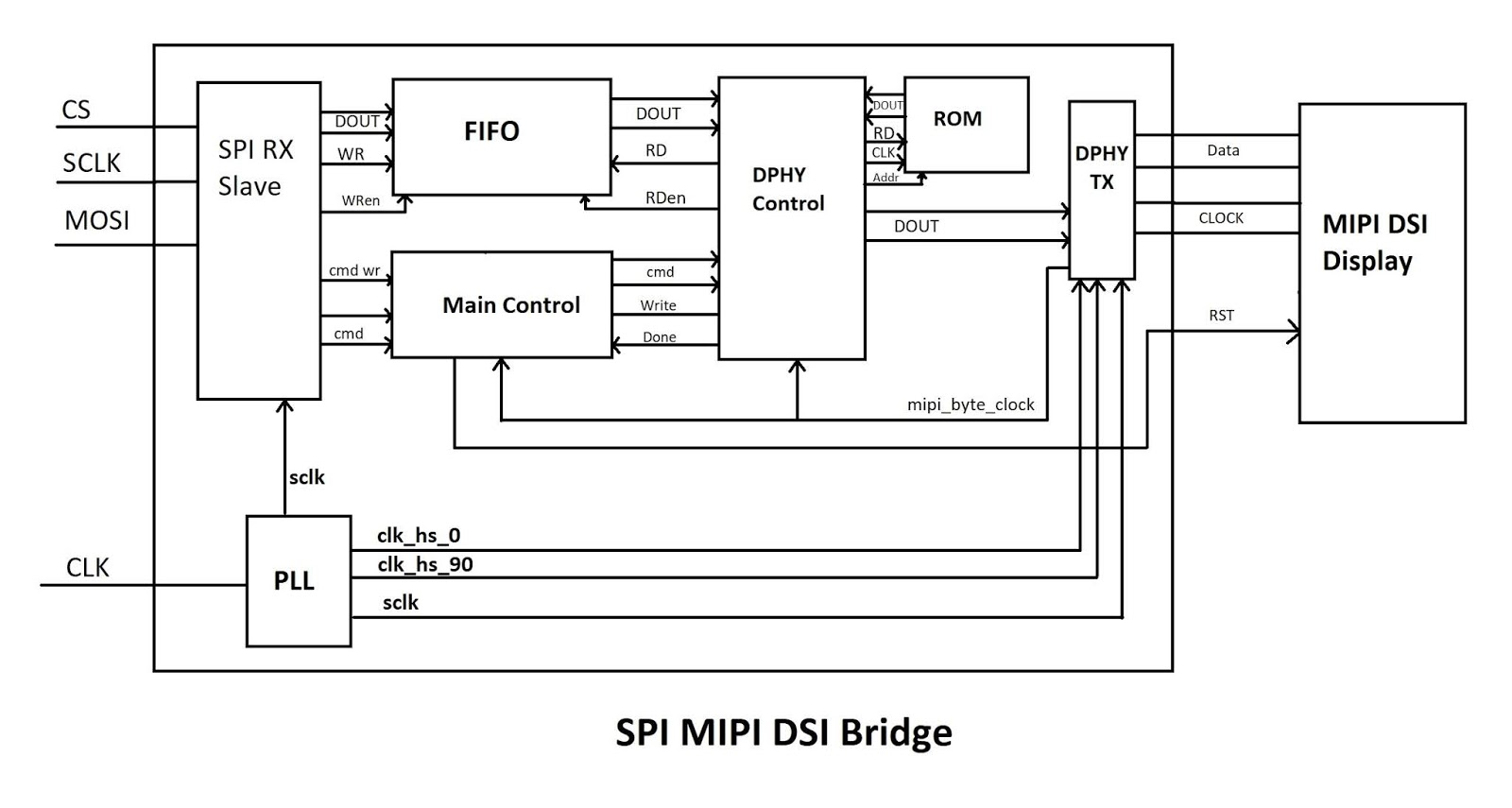
mipi_dsi_bridge.v file contains main control.
spi_slave.v file consist of SPI slave RX logic.
send_mipi_frame.v has DPHY control logic which also control ROM and FIFO Read operation.
pll.v has pll module.
rom.v has ROM initialized wit rom.mem rom file.
DDR_MIPI.V has my customized DDR element with LP bufffer.
Theory of Operation
System wake up from reset, LCD Reset control logic in the main control take over, Does correct power sequencing and with appropriate timings resets LCD.
One LCD is reseted , LCD get send initialization sequence with Display on command. Reset module waits for init finish. Then If requested also burst test pattern onto display From ROM.
ROM module store institutionalization sequence and other commands . ROM also store Test pattern.
Once initialization is done SPI waits for transfer from SPI master,
System is designed to latch commands and data from SPI. System is designed to send one complete MIPI HS line frame to display. Data is latched over one SPI frame line by line basis. master must transmit only one line per SPI translation. partial line will be padded zeros*.
Once Master start sending SPI CS activates FIFO write and everything received over SPI will be latched into fifo. SPI module also copy first byte off the transfer keep it as command and send into Main control logic once SPI CS deactivated.
Main Control module upon reception of command form SPI module send command to DPHY control module. and waits for signal from DPHY control for finish of TX.
DPHY control module is responsible sending one complete HS frame. DPHY control parses the command with help ROM , Generate HS-Entry sequence, sends needed preamble , sends ROM, if needed send FIFO content and finally finish it trail bytes. and Notify back to Main control once Transaction is done
PLL module generate three clocks , Two 90 degree phase difference fast clock for MIPI hs bit clock and one slow sync clock for both MIPI and SPI module.
All other module get fed by byte_clock generated by DPHY_TX module.
FIFO is 1024 byte long which can hold two lines,FIFO enables master to continuously send data while DPHY TX module is at the same time transmitting over to MIPI lines.
DDR TX BLOCK
I have customized this module a little when compare to standard ipexpress generated one. I have made changes to support TX only.

Simulation
Lattice Diamond comes with a version of ActiveHDL so i have used active HDL to simulate.
Testbench is written to simulate Reset , Init, Test Pattern and the finally SPI Frame write
 |
| ActiveHDL Simulation showing Reset -> Init-> Test Pattern-> SPI Frame write |
 |
| Reset and Initialization Sequence |
 |
| Initialization Sequence |
 |
| Start of First line Write of Test pattern From ROM |
 |
| Start Writing SPI Data into FIFO |
 |
| SPI Received data transmitted First line (From FIFO) |
 |
| End of Data Write |
USB Controller
To transmit images from PC to the display, I have Made PIC32 USB HS based USB to SPI Bridge with a QT5 Application running on PC. This post has gone too long so Details about USB controller and QT5 Application can be found in the next post.


Source Code
Verilog Source code andother files are availabe in github repo
Wow! Thanks for ur awesome project!
ReplyDeleteDear Mr. Gaurav. Your work is amazing. I would like to know, can you do any electronics development job by demand? If yes, please, send-me an e-mail on ifzq0@yahoo.com.br , I would like to quote with you to develop a hardware to my needs. Thank you!
ReplyDeleteThis is an amazing work obviously. Congratulations! I found a few things that might be a problem:
ReplyDelete1) TC2117-1.8VDBTR is used for U5 but VCCIOLP is 1.2V. The part should be updated I think.
2) 3.3V is used instead of 2.5V for LVDS25E. Lattice datasheet is not completely clear about that. I think it's still fine because it's differential. The main impact would be for the resistors with different values indeed? The schematics says that there is a calculator for the resistors values is in the source but i couldn't find it.
3) DDR_MIPI.v is not generated from DDR_MIPI_.ipx. I don't understand how this file has been generated. The commented header has some "false" information. This file is clearly coming form another ipx (perhaps a private Lattice ipx???)
4) The signal SYNC is at 3.3V but the screen IO is at 1.8V. In any case, it's not primary used.
5) For clarity, I think that BL_EN, REG_1V8 and REG_3V could be removed and forced to their ON values in hardware.
6) I'm wondering if the 96MHz clock needs to be very precise. Could it be for instance 95MHz and be generated with the internal oscillator (38MHz) + PLL (*5/2)?