From quite some time i have been working with different MIPI CSI Camera Solutions , Interfacing Camera with FPGA and Connecting to USB 3.0 Connection.
Board will be having USB C connector for USB 3.0 5Gbps Connection with Cypress FX3 CYUSB3014 and Lattice Crosslink FPGA
.JPG) |
| Board With Direct Raspberry PI IMX219 |
.JPG) |
| Board with FCP Connector for Any MIPI Camera With 1mm Flex cable |
.png)
Schematic
Both of the boards have similar schematic only Camera Section is different, First USB 3.0
USB Section has Cypress FX3 CYUSB3014 a generic USB 3.0 Controller with 32-bit GPIF bus for interfacing with ASIC and FPGA, This section of Schematic has USB C connector with its required protection and USB 3.0 Mux circuit. There is also oscillator and I2C memory USB Controller.
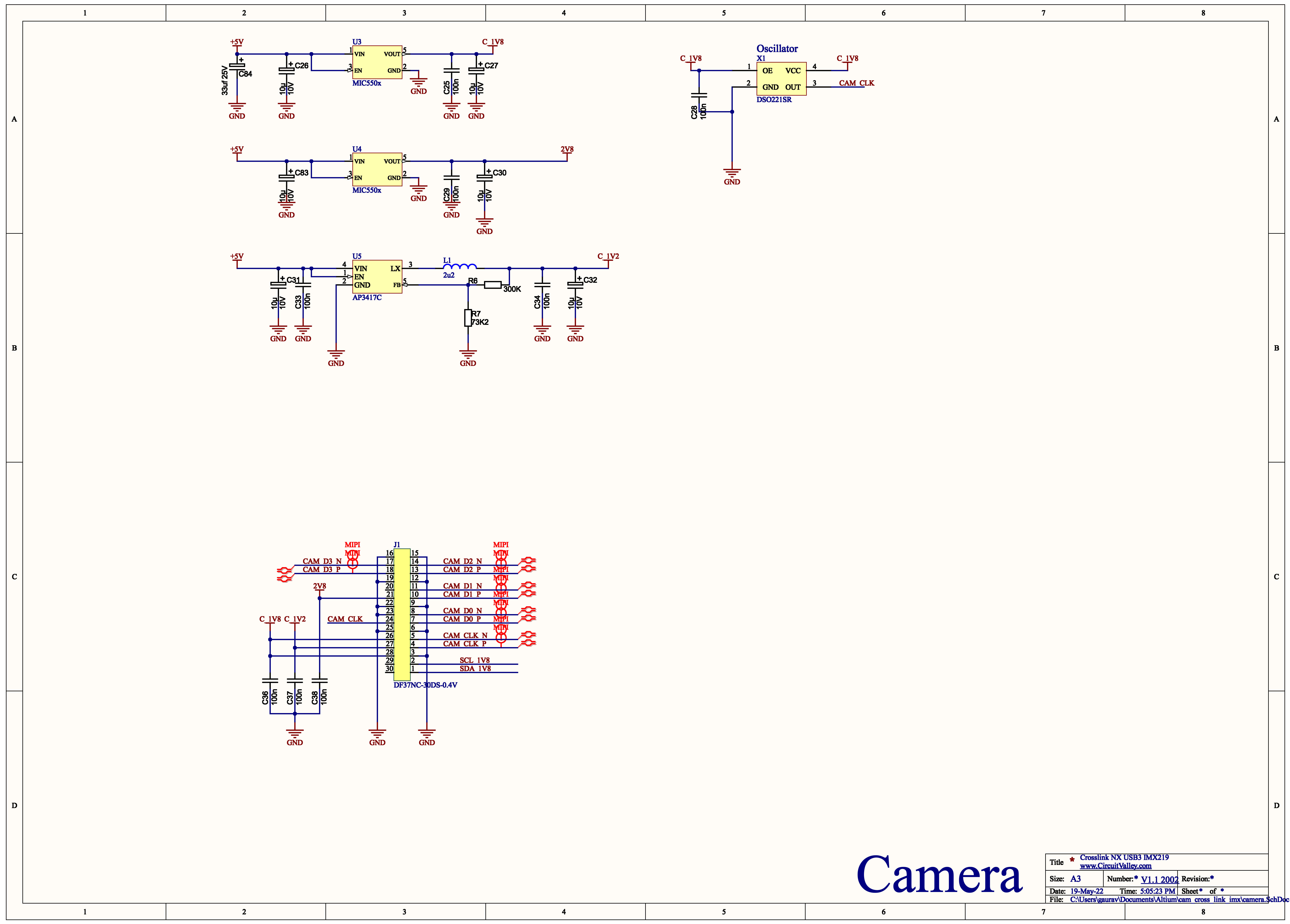
Power section has various switching regulator for FPGA and USB Controller also for Camera.
FPGA I am using is Lattice Crosslink NX LIFCL-40 , I have received quite a few of these from Lattice as early engineering samples. Though because of being engineering sample, these devices were having few bugs which caused quite a bit of trouble in this project. For example, All JTAG pins can only be used for JTAG and could not be used for other purposes even when JTAG is disabled. As my project needed almost all the the pins which Crosslink NX has to offer for 32-bit GPIF port of USB Controller, I called this project not complete success because I needed to implement quite a few work around even to get it working. All the Problems with these board are listed at end of the project.

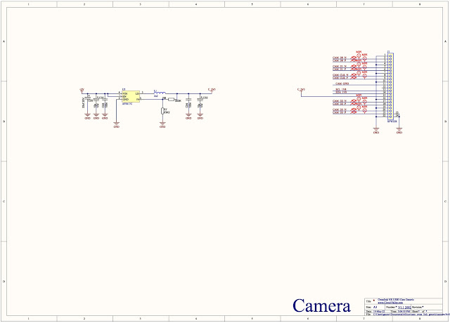
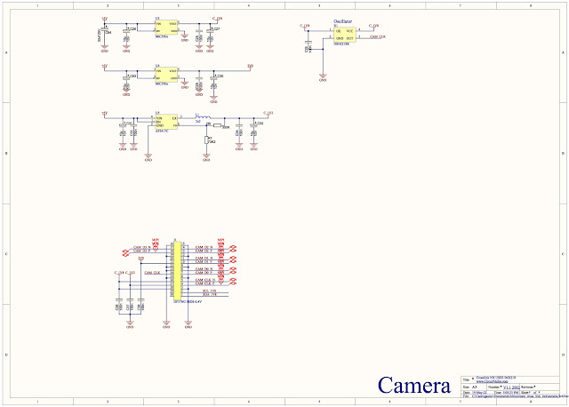
Camera Section for both the board is different, Though board board use 4 Lane MIPI CSI interface what Crosslink has for offer. One board has direct connector for IMX219 while other board has 22 Pin 1mm FPC connector which can accept both 15 Pin 2 Lane MIPI Standard Raspberry Pi style camera and also any custom 22 Pin 4 Lane MIPI sensor.
 |
| Camera section of Generic FPC Connector for external Camera modules |
 |
| Camera Section of Dedicated IMX219 Camera sensor |
PCB
Board is 6 Layer board with Layer stackup of Top Signal - GND - Power - Internal Signal - GND- Bottom Signal.
Clearance for top Layer is 0.09mm while minimum trace is also 0.09mm , Clearance on internal layer is 0.127 and minimum trace is also 0.127mm
.png) |
| Top Layer 1 of 6 |
.png) |
| Top Ground Plane Layer 2 of 6 |
.png) |
| Power plane Layer 3 of 6 |
.png) |
Internal Signal layer 4 of 6
.png) | Bottom Ground Layer 5 of 6
|
|
.png) |
| Bottom Signal Layer |
.png) |
| Top Signal Layer 1 of 6 |
.png) |
Bottom Layer 6 of 6
|
FPGA Firmware Design
If you want to know more in details how MIPI CSI work you can refer to my previous posts and my previous make of USB 3.0 Camera. Previous post discuss in very details how MIPI functions.
FPGA Design can be summarized in the blog diagram blow. Previous Project form post above discuss this in details
.JPG)
Byte Aligner Received Raw unaligned bits from DDR RX module outputs Aligned bytes, Bytes on MIPI lane does not have any defined byte boundary so this modules Looks for always constant first byte 0xB8 on wire, once 0xB8 is found, byte boundary offset is determined, set output valid to active and start outputting correct bytes stays reset when data lane are in MIPI LP state
Lane Aligner Receives multiple lane, byte aligned data from mipi rx byte aligner @mipi byte clock outputs lane aligned data in a multi-lane mipi bus, data on different lane may appear at different offset so this module will wait till of the all lanes have valid output start outputting lane aligned data so byte x from all the lanes outputted at same timescale
MIPI CSI Packet Decoder Basically a packet Stripper, removes header and footer from packet Takes lane aligned data from lane aligner @ mipi byte clock looks for specific packet type, in this case RAW10bit ( 0x2B). Module outputs Stripped bytes in exactly the way they were received. This module also fetch packet length and output_valid is active as long as input data is valid and received number of bytes is still within the limits of packet length.
MIPI CSI RAW10 Depacker Receives 4 lane raw mipi bytes from packet decoder, rearrange bytes to output 4 pixel 10bit each output is one clock cycle delayed, because the way , MIPI RAW10 is packed output come in group of 5x40bit chunk, output_valid_o remains active only while 20 pixel chunk is outputted
Debayer / demosaic Takes 4x10bit pixel from RAW10 depacker module @mipi byte clock output 4x24bit RGB for each pixel , output is delayed by 2 lines Implement Basic Debayer filter, As debayer need pixel inform neighboring pixel which may be on next or previous display line, so input data is written onto RAM, only 4 lines are stored in RAM at one time and only three of the readable at any give time , RAM to which data is written to can not be read. As we have enough info in RAM 4 10bit pixel will be converted to 4x24bit RGB output First line is expected to BGBG , second line GRGR Basically BGGR format
RGB to YUV Color Space Converter Received 4 pixel 120bit RGB from the Debayer filter output 64bit 4pixel yuv422 Calculation is done based on integer YUV formula from the YUV wiki page
Output re-formatter Takes 64bit 4pixel yuv input from rgb2yuv module @ mipi byte clock outputs 32bit 2pixel yuv output @output_clk_i , output_clk_i must be generated by same way as mipi byte clock, output_clk_i must be exactly double to mipi byteclock This implementation of Output reformatter outputs data which which meant to send out of the system to a 32bit receiver depending on requirement this will be need to be adapted as per the receiver
Issues with board and Crosslink NX Engineering Sample chips
As this board is made with Engineering sample only 72 pin Crosslink NX LIFCL-40 device , it had its fair share of limitations, most of which only caused by Crosslink NX LIFCL-40 being in 72 PIN QFN package.
So here are the limitations which makes both the boards basically very limited.
I needed to use every single pin that is available on this part for 32bit GPIF port of Cypress CYUSB3014 , Crosslink allow muxing of few pins but few limitations were there.
1. JTAG EN Pin basically does not have any effect on JTAG pins, JTAG pins are stuck on JTAG function if you powered on the part with JTAG enabled and programmed the device once. So 4 of the pins are just not available on the device if you used JTAG. This a silicon bug i hope fixed in production version of Crosslink NX
Work around for this problem is load firmware directly to external Flash and on next power cycle FPGA will load firmware directly from Flash to its memory and JTAG pins would be available.
2. Few more pins like PROGRAMN , INTN , DONE pins are also same which are stuck on there respective function even though from Radiant Software I put in bitstream that these pins should be available as pins that firmware can control. This is bug in Radiant software and Silicon
Work around for this problem is , Lattice radiant allow a sperate Feature bit programming which enables normal IO function on Special function pins, But again there also bug in Crosslink nx, Though these bits should be permanent even after power cycle, in real hardware they only stay active for one power cycle, and to program them you need JTAG , using JTAG disables JTAG pins for this session.
3. This problem is with loading bitstream from external flash, FPGA suppose to load bitstream on every boot, but it does not work.
work around for this problem is to use a button PROGRAMN pin to force load bit stream.
4. Problem described above are problems related to Crosslink NX or Lattice radiant software. This problem is more specific to IMX219 board. When board power up IMX219 expects a reset/appropriate power cycle but it does not happen as i do not any connection to the IMX219 power enable or to reset.
Workaround for this problem is to disconnect and connect camera after every power cycle.
As said problems mentioned above make this board quite limited you can possibly get around most of them, or even use 24 bit or 16 bit but FPGA issues are really make it hard for real product, I hope issues are limited with engineering samples and not with production Crosslink NX chips
Project Source All source can be found on Github , here on the link blow.

.JPG)
.JPG)
.JPG)
.png)
.png)
2.JPG)


.png)
.png)
.JPG)
.JPG)
.JPG)
.png)
.png)
.png)
.png)
.png)
.png)
.png)
.png)
.png)
.png)
.JPG)
.JPG)
.JPG)
.JPG)
.JPG)
.JPG)

Comments
Post a Comment