Making Opensource USB C industrial camera with Interchangeable C mount lens, Interchangeable MIPI Sensor with Lattice Crosslink NX FPGA and Cypress FX3 USB 3.0 controller
This post is going yet another part in the DIY camera projects which have been doing since quite some time. In this post I will showing you next successful implementation of making C mount high lens mount USB C camera. This implementation will have absolute modular boards having dedicated Sensor board which can be changed if needed.
Hardware System
There are three boards, USB, FPGA and Sensor board.
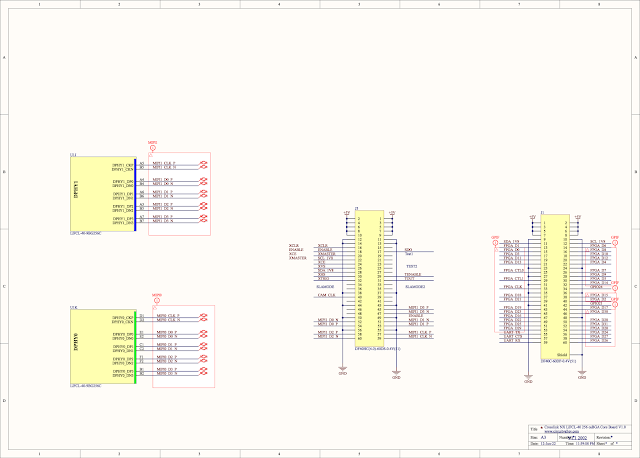
Sensor board has Sensor itself along with its power and Oscillator, Board has High Density connector to be able to connect to FPGA/Host board, High Density connector also supply power to the board has I2C, 4Lane MIPI with clock , I2C and also few other control signals.
Currently I have just one camera PCB, This schematic shows IMX290 IMX327 IMX462 PCB , all these 3 sensors have same resolution and also same PCB footprint.
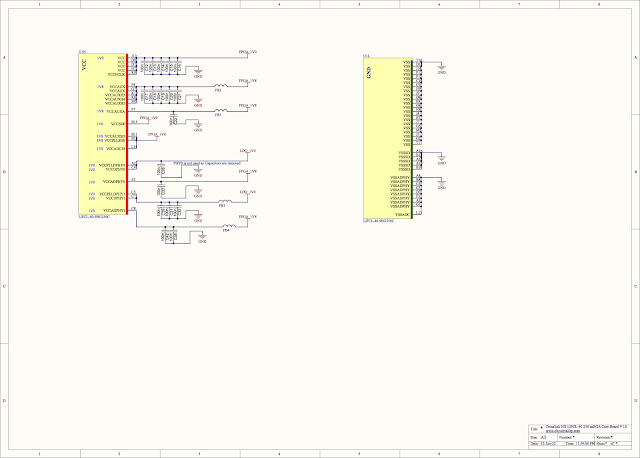
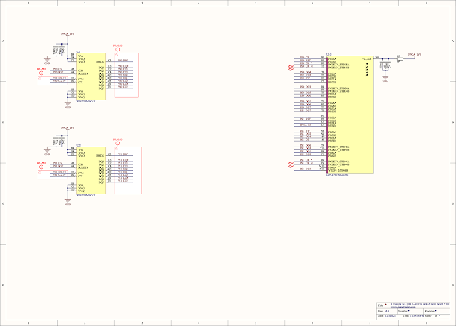
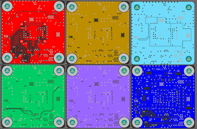
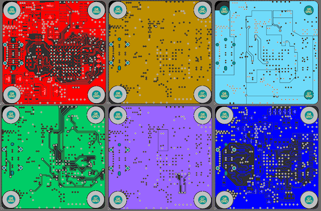
FPGA board
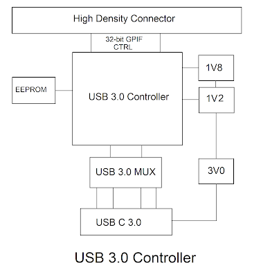
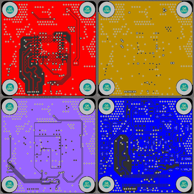
USB 3.0 board
All of the boards are 6 Layer, All of them are 27 x 27 mm , while mounting holes are 22 mm appart
Camera sensor Board
USB 3.0 Board
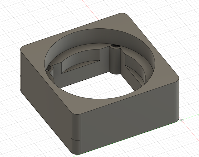
To be able to mount a C mount lens I designed a mount in Fusion 360. as small threads on FDM printer are little hard to deal with There are many already made aluminum CS mount to C mount adapters are available online, Raspberry Pi camera also comes with one such ring, I bought these CS to C mount ring and I designed part around my PCB to fit these CS mount adapter ring to give me metal thread.
FPGA Design
MIPI
What is MIPI, you can google it to find out but basically it is a interface specification for Displays and Camera sensor to a application processor.
Image blow show block diagram of MIPI. On one side there is application processor and other side is the peripheral. When peripheral is Camera and CSI apply. though mipi is closed specification which means one has to be member of MIPI consortium to gain access to full specification. And membership of the consortium comes with a big price tag for individuals. Luckily full specification is already available just a right keyword web search away. DCS, CCS, DSI, CSI and DPHY all the specification are available with just few minutes of web search.
MIPI DPHY Signal
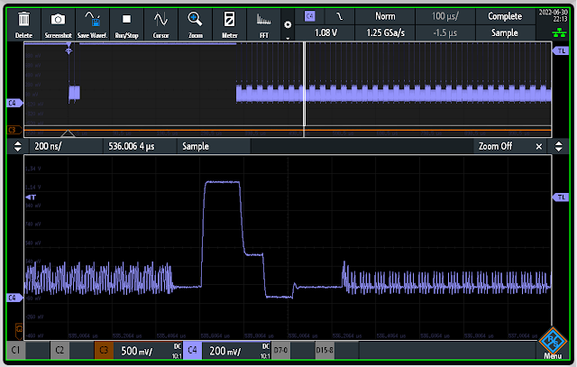
The image shows i got from google shows signal level for MIPI , HS driven by differential driver swings -200mV to +200mV at offset of 200mv. while LP signal is a 1.2V lvcmos
there are two different modes of transmission , HS mode and LP mode, HS mode is for hi speed display data while LP mode is for Low power transmission.
Receiver must detect when transmitter has gone into HS mode and exited HS mode.
Image blow shows how transmitter enter HS modes.
Stage 0 : LP-11 state in the shown image is LP state.
Stage 1 : To get into HS mode driver drives LPdp low for Tlpx(minimum 50ns) and stay in LP-01 (HS driver is tristate in LP 01).
Stage 2: Driver drives LPdn low for Ths-prepare (minimum 95ns) stay in LP-00 , Later somewere in the middle of this stage target device will activate it's 100R termination register.
Stage 3: Now Target is in HS, driver activates HS driver start sending mandatory zeros .
Stage 4: Send mandatory 0xB8 sync byte and then payload.
CSI
As explained earlier CSI , describes Packet structure. How exactly bytes are packed on to wire in different lanes configuration.
Image blow shows packet structure.
There are Two types of Packets
Short Packet: 4 Bytes (Fixed Length)
Long Packet: 6 - 655541 Bytes (Variable Length)
 |
| MIPI Short Packet Structure |
 |
| MIPI Long Packet Structure |
Endianness
Bytes are sent lsbit first and bytes in the packet are sent LSByte first.
CCS
Very important fact with CCS when comparing with DCS , CCS describes command interface to be I2C while with DCS commands are set over same HS line as the data itself.
But in case of camera as per MIPI spec CCS is implemented over a extra I2C line.
CSI Single Frame
Single Frame from camera is show in the image blow.
Camera send a Frame start packet
Then send embedded line information which tells receiver about the stream
Then image data line by line.
Test Video
What make this camera sensor different to camera modules
IMX219 camera is bare bone camera sensor. What do means when i say bare bone camera sensor is , there not much image processing going on on the camera die it self. Camera sensor is Sensor array with Bayer filter on it , 10 bit ADC , clock system , MIPI output driver and I2C controllable system control.
What does this means for us as camera sensor implementer. As my final goal is to interface this camera to USB3.0 UVC with RAW YUV. This camera does not output YUV, forget about YUV this will not even output RGB. Camera output is absolute RAW 10-bit ADC conversion result from the Bayer filtered sensor array.
So go first get RGB output from bayer raw data, a Debayer or demosaic need to be performed. Once demosaic is done we will have RGB ready to be converted to YUV. And one we have YUV it can be transmitted to USB to be displayed.
What next this camera will not have is any automatic control over exposure. because camera does not have any intelligence to know how dark or bright scene is. Solution to this problem what raspberry pi implement is , Raspberry Pi regularly on each frame update analog gain register over I2C to adjust gain according to how bright and dark scene is.
This camera does not have any white balance control as well so host must do correct while balance compensations. To get correct colors out of image.
FPGA module Block Diagram
FPGA block diagram is show in the image blow. This diagram describe how overall system is implemented and what the key components what this diagram does not describe is control signals and other miscellaneous stuff.
Byte Aligner Received Raw unaligned bits from DDR RX module outputs Aligned bytes, Bytes on MIPI lane does not have any defined byte boundary so this modules Looks for always constant first byte 0xB8 on wire, once 0xB8 is found, byte boundary offset is determined, set output valid to active and start outputting correct bytes stays reset when data lane are in MIPI LP state .
Lane Aligner Receives multiple lane, byte aligned data from mipi rx byte aligner @mipi byte clock outputs lane aligned data in a multi-lane mipi bus, data on different lane may appear at different offset so this module will wait till of the all lanes have valid output start outputting lane aligned data so byte x from all the lanes outputted at same timescale
MIPI CSI Packet Decoder Basically a packet Stripper, removes header and footer from packet Takes lane aligned data from lane aligner @ mipi byte clock looks for specific packet type, in this case RAW10bit (0x2B) RAW12bit (0x2C) RAW14bit (0x2D). Module outputs Stripped bytes in exactly the way they were received. This module also fetch packet length and output_valid is active as long as input data is valid and received number of bytes is still within the limits of packet length.
MIPI CSI RAW Depacker Receives Upto 4 lane raw mipi bytes from packet decoder, rearrange bytes to output upto 8 pixel upto 16bit each output is one clock cycle delayed, because the way, output_valid_o remains active only while chunk is outputted
Debayer / demosaic Takes upto 8x upto 16bit pixel from depacker module @mipi byte clock output upto 8x upto 32bit RGB for each pixel , output is delayed by 2 lines Implement Basic Debayer filter, As debayer need pixel inform neighboring pixel which may be on next or previous display line, so input data is written onto RAM, only 4 lines are stored in RAM at one time and only three of the readable at any give time , RAM to which data is written to can not be read. First line is expected to BGBG , second line GRGR Basically BGGR format
RGB to YUV Color Space Converter Received upto 8 pixel RGB from the Debayer filter output upto 8pixel yuv422 Calculation is done based on integer YUV formula from the YUV wiki page
Output reformatter Takes upto 8pixel yuv input from rgb2yuv module @ mipi byte clock outputs 32bit 2pixel yuv output @output_clk_i , This block has RAM to have output clock independent of mipi clock, Output clock_clock must be fast enough to be able to get whole line worth of data before next line starts, This implementation of Output reformatter outputs data which which meant to send out of the system to a 32bit receiver depending on requirement this will be need to be adapted as per the receiver
Debayer / demosaic Need little more attention than other modules , IMX219 datasheet incorrectly mention output as to be either GBRG or RGGB.
But after wasting lots of time it turned out camera output BGGR . IMX219 Camera only output BGGR as defined by the IMX219 Driver in linux repo MEDIA_BUS_FMT_SBGGR10_1X10, Camera datasheet incrorrectly defines output as RGGB and GBRG. Data sheet is incorrect in this case.
To test my debayer, Iwas using built in camera test patterns. One key thing about IMX219 is Bayer filter type does affect test pattern as well. It seems like in Test pattern mode it outputs RGGB instead of BGGR. Test pattern will have R and B channel inverted when image have right color.
Update: I have discussed this issue with raspberry pi , It turned out flipping image seems to be the solution, once image flipped bayer output it correct for both data from sensor and test pattern. because flipping image does not affect bayer order of the test pattern.
MIPI RAW Packet Format
ISP Pipeline Specifications
No virtual restriction on supported frame rate or resolution. Tested more than 4K with IMX477 4056x3040. Can do 8K with around 30FPS or even higher than that as long as FPGA is fast enough for needed frame rate and FPGA/Board has enough memory to be able to store minimum 4 Line worth of pixels. Output Clock is independent of MIPI clock. Easily Portable code to Xilinx or any other FPGA, No Vendor specific components has been used except for the PHY itself which can be replaced by other vendor's DDR phy and Embedded Block RAM. Only Debayer/Demosaic and Output reformatter need Block RAM. Block ram can also be replaced vendor's RAM. Auto detection of RAW pixel width supporting different camera sensors and sensor modes without FPGA reconfiguration.
Speed
- Supports MIPI bus clock 900Mbitsps Per lane with upto 4 Lanes, Total 3.6Gbitsps Sensor bit stream, Has been Tested upto 900Mbitsps with 8x Gear.
- Pixel Processing pipeline with 2,4 or 8 Pixel per clock can reach more than 110Mhz with Lattice Crosslink-NX LIFCL-40 High Speed, So basically Can process upto 880 MegaPixels per second. With this can reach Around 120FPS with 4K resolution and around 30 FPS with 8K. Or even 3000 FPS with 640 x 480 as long as Camera and MIPI Wire allows. With Different Faster FPGA speed will be more.
- FPGA Oputput Pipeline is decoupled from MIPI clock, runs on output clock, It feeds into Cypress FX3 32bit GPIF can do Max 160Mhz. Cyress FX3's specs limits max GPIF clock to 100Mhz.
Configurability
- Selectable max RAW pixel width
FPGA Design is configurable with parameters to support pixel depth from RAW10 to RAW14 or Virtually any bit depth even 16bit RAW when it becomes a MIPI Specs. Parameter specify maximum pixel width that is supported while module auto detect package type at runtime with RAW14 selected as max pixel width, RAW10, RAW12 and RAW14 will be automatically detected and processed
- Selectable number of MIPI lanes: With just definition of Parameter value number of lane is also configurable between 2 or 4 MIPI lanes.
- Selectable Pipeline Size: Pipeline is Configurable with a parameter to Process 2,4 or 8 Pixel. 2 Pixel Per Clock is only available with 2 Lane MIPI, while 8 Pixel Per Clock is only available with 4 Lanes.
- Selectable MIPI Gear Ratio: User can select weather to operate MIPI/DDR Phy in 16x or 8x Gear ratio. Most DDR/MIPI Phy supports 8x Gear while few do support 16x gear.
- Selectable MIPI continuous clock mode
User and select between MIPI clock lp based Frame sync or Frame start and frame stop packt based frame sync. Some MIPI cameras do not support going to LP mode while frame blank occur, With this option user can enable Frame Start and Frame stop detection, to have a frame sync. - Selectable ROM based Sample Generator
For ISP debuging ROM based sample generator can be activated. Two ROM lines are there have both even and odd line to full image test.
Block RAM and DDR PHY IPs need to be manually regenerated if Gear, pixel width , lane or PPC is changed.
Tests
4 Lane 12 bit IMX477
4056x3040 20 FPS Full Sensor
2028x1520 70 FPS Full Sensor Binned 2x2
2028x1080 100 FPS
4 Lane 10 bit IMX477
1332x990 200 FPS Binned 4x4
640x480 400 FPS Binned 4x4
2 Lane 12 bit IMX477
4056x3040 10 FPS Full Sensor
2028x1520 35 FPS Full Sensor Binned 2x2
2028x1080 50 FPS
2 Lane 10 bit IMX477
1332x990 100 FPS Binned 4x4
640x480 200 FPS Binned 4x4
2 Lane 10 bit IMX219
3280x2464 7 FPS
1280x720 30 FPS
1280x720 60 FPS
1920x1080 30 FPS
640x480 30 FPS
640x480 200 FPS
640x128 600 FPS
640x80 900 FPS
4 Lane 12 bit IMX290/IMX327/IMX462
1280x720 120 FPS
1920x1080 120 FPS
2 Lane 12 bit IMX290/IMX327/IMX462
1280x720 60 FPS
1920x1080 60 FPS
What decides camera Max FPS
Camera timing is controlled by just a few registers which control Clock. Then every sensor has a maximum ADC sample rate to convert Pixel Value to Digital, Different camera sensors have fast or slow ADC. or even multiple ADCs. so you do simple division on what your ADC pump needs for the needed frame rate. Shutter open time is also user adjustable so that also affects frame rate. And Interface clock is also important, If ADCs faster than how fast interface can pump data out of sensor then you have an issue of FIFO full.
Scope capture
.png) |
| MIPI 2 Lane Mode, Decoded Data shows both lanes of lane aligned data IMX219 Full frame one of the line, on ch2 is byte clock |
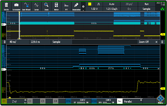 |
| A start frame MIPI package (0x00), Use for Frame Sync with cameras where Clock does not go into LP during frame blank |
.png) |
| A Frame Stop MIPI package (0x01) , Use for Frame Sync with cameras where Clock does not go into LP during frame blank |
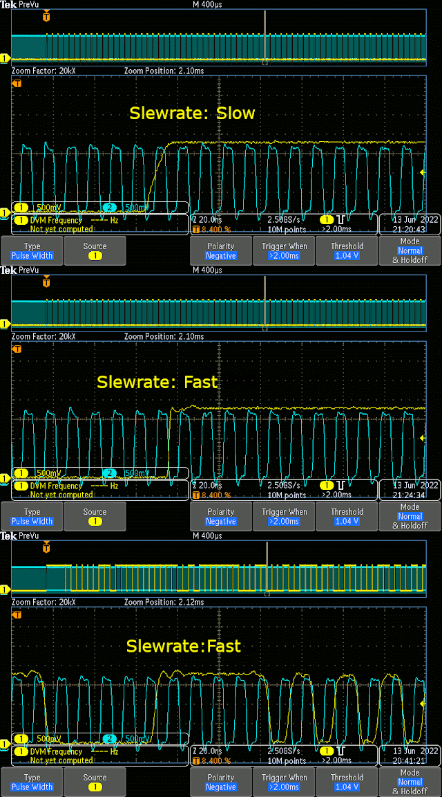 |
| Show difference of Fast vs slow slew rate on GPIF port , CH1 shows GPIF port data line and ch2 is ~100Mhz clok |
Test image
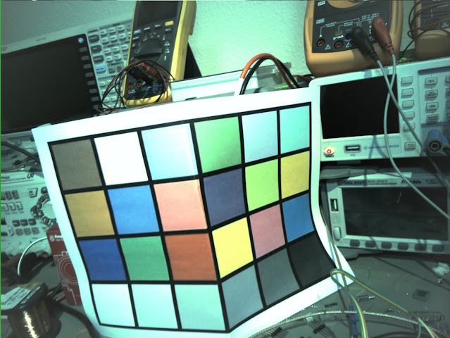 |
| IMX219 Basic Test Full Frame Colors Uncorrected |
 |
| IMX219 Full Frame Test pattern 5 |
 |
| IMX477 Full Frame Test Pattern 2 |
 | |
|
Cypress FX3 Firmware
Firmware implementation with FX3 was quite easy. I have put all the resolution and framerate in the USB descriptor , As described earlier this type of camera sensors are quite bare bone all the have sensor element, PLLs and ADC . So this camera sensor does not have any control over exposure, White-balance or even brightness, I have implemented manual control over USB UVC control channel. it possible to completely control camera exposure and brightness.
Few things you keep in mind, cypress fx3 clock frequency need to be set in 400Mhz mode to allow full 100Mhz 32bit GPIF DMA transfer.
One more thing is though Cypress CYUSB3014 has 512KB RAM but only 224 KB and additional 32KB is available for DMA buffer.
Having large buffer chunk is really important because on every DMA chunk CPU intervention is expected to insert UVC header. As this is high performance application less often CPU intervention is needed is better. So I have set DMA chunk / UVC individual packet to 32KB
Scope capture Image blow shows Channel 13 is the individual DMA packet capture and on Channel 12 show CPU DMA finish interrupt.
These Two scope capture show difference between 16KB DMA vs 32KB DMA
 | |
|
 |
| 32KB DMA Size, CH13 DMA packet , CH12 CPU interrupt |
PCB and Schematic Source is available in the Github Repo.
https://github.com/circuitvalley/USB_C_Industrial_Camera_FPGA_USB3
2.JPG)
24.JPG)


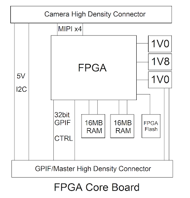




.JPG)
.JPG)

.JPG)

.JPG)
1.JPG)
1.JPG)
2.JPG)
.JPG)
.JPG)
.JPG)
.JPG)
.JPG)
.JPG)
.JPG)
.JPG)
.JPG)
.JPG)
.JPG)
.JPG)
.JPG)
.JPG)
.JPG)
.JPG)


Absolutely interesting! Very good job! Thanks for share!!
ReplyDeleteVery Impressive!
ReplyDeleteHi !
ReplyDeleteThe project is super !
Is it possible to add an imx335 industrial sensor to the project ?
IMX335 is also MIPI CSI sensor, So it can be added, I just did a quick search and found sensor itself is not available for purchase but you can buy IMX335 based cameras pretty cheap and get camera sensor out of it. Yes you can have IMX335 As long as you have sensor and Sensor PCB for it.
DeleteAny intentions to support any of the global shutter IMX modules?
ReplyDeleteThere noting special need to be done to support any new MIPI sensor.
DeleteAs long as i could lay my hand on the sensor or even Raspberry Pi style camera module. I could integrate driver into USB part and its done.
Do you have any suggestion of any easily available sensor?
DeleteExcellent,Is it possible to scale for other Humidity, measuring and texture and servo motor control sensors?
ReplyDeleteDo you have any specific part number in mind, I assume Humidity sensor would not generate enough data to justify use of an FPGA
DeleteI haven't any idea about parts .
ReplyDeleteBut our target is to building of hyperspectral cameras the near-infrared
- 900 – 1700 nm
-SWIR (1000 – 2500 nm)
- (2700 – 5300 nm) spectral range .
These wavelengths are part of the thermal range, so-called MWIR.
the targets’ chemical composition for analysis, or detect moisture or foreign objects in the target. For instance, it should can be used to detect the sugar level on berries or potatoes or moisture percentage on baked goods, or to identify different plastic types for recycling.
Please advice.
Sorry for delayed response, I Have few questions before i could possible answer your question. Is this near infrared camera sensor a normal camera sensor with specif filters or specific filters removed a normal camera sensor?
Deleteit is normal camera sensor then you do not need to do much.
But if it is special camera sensor but has MIPI CSI 2 as interface and Does output mipi RAW style format, then also you can pretty much use design as it.
But if you have special camera with LVDS, Parallel or SLVS-EC then you need some modification to hardware and software.
If you are talking about specific solutions then you have to talk about what exactly you are dealing with.
You need a special SWIR sensor (usually cooled) and very expensive special lens for anything greater than 1100nm. Not cheap.
DeleteHoly Sh*t... this is incredible. You should seriously write a book for serious hobbyist to build such advanced cameras from scratch as like what you have did.
ReplyDeleteWould like to congratulate you for such remarkable DIY camera build you made.
I have been searching on google for tutorials on how to build cameras from scratch and couldn't find any. Luckily I found this tutorial.
Thanks for this great DIY documentation.
Hi ,
ReplyDeleteCan i ask one thing? Sorry i am not familiar with fpeg.So my question may sound silly...
Why you don't consider cypress cx3? Using cx3 as bridge and connect with sensor via 4 lane. Is it more easily to archive then your way?
Why you need FPGA and cypress-fx? It is more difficult to study and make thing goes well as i think…
And cognation! good work.
My company is producting ccm camera and usb camera/
Current our compnay is using other company's product to test mipi 4 lane sensor. It’s bandwidth is 2.5Gs/s.
I ask because my boss want us survey how to build our own tester for saving money and for me, I can learn skill which is fun fo me.
So i have 3 opions , I do not know which is beter, can you give me some advice?
1 jetson nano/rpi cm4 + sensor transfer board + custermor sensor board.
: Mipi protocol + usb protocol+ linux driver + open source mipi 2 lane codes(I can not found 4 lane source code for now)
2 cypress cx3 + sensor transfer board + customer sensor board.
: Mipi protocol + usb protocol + cypress sdk
3. Like your demo
Lattice Crosslink NX FPGA+ Cypress FX3 USB 3.0+ sensor transfer board + customer sensor board.
: Mipi protocol + usb protocol + FPGA+ cypress sdk
Thanks in advance
Terry
Primary difference between FX3 and CX3 in this application would be, Solution FX3 + FPGA will not need any custom application at the PC side. Solution with FX3 implements standard UVC device. As UVC does not support RAW or RGB so solution with CX3 would need to implement a custom application/driver solution on the PC side. As almost all of the MIPI CSI-2 Camera only output RAW bayer. RAW bayer need to be converted to useable format before anything can be done with it.
DeleteAll three possible solution have few limitations and also few advantages.
1. With Jetson or RPI , Easy to make will be for sure, Why would really need all 4 Lanes? 4 Lanes "May" give just few more FPS. a custom Jetson board will support 4 Lanes camera, Or a Raspberry Pi module also support 4 Lane camera. Latency may be an issue depending on how you using it and also because image has to go throw whole Linux ISP.
2. Cypress CX3, Will need custom driver and/or custom application on the PC/USB host side. If you are under windows getting driver signed and even driver development on windows may not be as fast.
3. Has really good latency, Cost is high but still less than a Linux SBC, Has few limitation with Image quality and corrections.
Regards
Hello,
DeleteThanks for your replay. We need 4 lane jig because our customer need 4 lane. and In our firmware engineer said, if we want use 2 lane to archive the same fps as 4 lane. The clock must be higher twice clock rate more then 4 lane. It is easier to cause problem.
And Currently I think Way 3 is more good for us. Beause the mipi bandwidth. Currently Our customer use 16m 30fps. I think in the future they will use more bandwidth(Maybe 20M or 32M 30fps).
Lattice CrossLink-NX is 2.5g per lane. Cypress Fx3 is 5g/s. In the future, we can use Sx3 to get 20g/s.
Terry
Hello ,
ReplyDeleteanother question:how to build your lattice crosslink nx ffpeg firmware?
Is it using lattice diamond software? I ask become i can not find project .only .v verilog file..
Thanks in advance
Terry
Lattice Crosslink nx are supported by Lattice Radiant software, Not by Diamond, You need to create a lattice radiant project, Chose target device, Add all v files and also from Lattice Specific folder under src all IP v files then, implement
DeleteHello,
ReplyDeleteMy goal is try to use your project and try to understand. If I use your project and try to light another mipi 4 lane sensor(like ov13b10 , or ar1335 just for example, is it very difficult?
I use Lattice Radiant , Create a project(Terry_test_crosslink_nx) ,and Use your src/*.v and Lattice_specific/*.v, I Choose LIFCL(CrossLink-NX) ,(I guess from your pic.) and Run All. And it seems work without Error but warning. And when I click Netlist Analyzer some thing think schematic shows.
How do I know the output is ready? What is the ouput of FPGA. Sorry I ask the silly problem...Is it Terry_test_crosslink_nx_impl_1.ibs? I found it in IBIS directory.
If I can produce the FPGA code, and cypress fx3 code, next stage is try to make our hardware to see your Hardware and try to make one for test purpose.
My boss told me it is very difficult for me cause I am not fpga Engineer, I said I want to use your project code and try to adjust it. Also FPGA have ip,I know I am beginner in FPGA, but I think it is possible for me to change your code for our customer ccm boad.(With vcm possible), and write cypress firmware . For PC write AP use UVC extension to issue I2c and get raw data from fx3 and fpga .
I am not FPGA programmer, I have only a little Hardware background( Nmos, Pmos, PNP, adc,capacity a little knowledge) I use Stm32 and pico in the past as Jig, use I2c to commute with Our Lighsensor / Hall sensor and to test it in producing line. Also some knowleage of linux driver.(I use open uvc linux driver and change it for our customer module about 5 years, I can only modify it, I can not write my own uvc linux driver by myself.)
I am a software Engineer for about 20 years., my main focus is c/c++/ OpenCV / Microsoft MFC/algorithm, I graduate at Mathematic degree and got Computer Science master degree. So my hardware is weak. Currently I study MIP/PHY spec and USB spec for this purpose. Also try to learn Verilog . I like to study. That is why I am willing to tough this area. The question is if I will take too much time to archive.. My boss won’t got happy if I need one year or longer to do it : )
Terry
You would have bit file as output. That file can be programmed on FPGA.
DeleteI have an old project published which uses Off the self development boards, One from lattice mach XO3, another one Cypress FX3 USB board. If I am starting I would use that to begin with.
Hello,
ReplyDelete1. Can i ask one thing, if i want bought sensor/ FPGA /fx board from you. Do you have this product for sale?
2. How can i burn FPGA in your board? I know i can burn FPGA from usb or jtag if i buy lattice crosslink NX demo board. But i do not know how to burn FPGA code if from your FPGA board.
3.I plain to make our hardware product from your Gerber, But i am afraid some thing will go wrong. That's why i want buy product from your side directly. And when i have ability to understand your code. I will make our hardware product from your Gerber and schematic.
4. We ask lattice agent in Taiwan. They said the MIPI IP need 5000 license fee. Yet i can test for 4 hour each time. It is enough for me. Is it also the same in your board?
5. I try to search FPGA + usb 3.0 solution. Currently only your poject can do it, that is why i am urgent to look for your help.
6. Please correct me if i am wrong cause i am a beginner in FPGA...
Thanks in advance.
Terry
1. Depending on your use, I may have few boards left.
Delete2. There is Flash memory on the board, Once firmware is flashed you do not need any programmer, To reprogram you would need any FT2232H cable, I have used busblaster and few other generic FT2232H board.
3. You can possibly order board and try to solder them self. You would need to take a little care with as board has Large Fine pitch BGA.
4. I do not use any IP from Lattice that need any fee. I use dphy IP as without using it you just can not use hard DPHY of crosslink nx. That IP is free, It is just basic building block. You can even avoid using that if needed to.
6. It is some what complicated project for beginner to approach, I hope you can understand.
Regards
Hi Terry, Have you successed programed the FPGA? I use the HW-USBN-2B do not successed.
DeleteHello,
ReplyDeleteSorry for the late response. And thank for your kindly response! I see your message 9/26 and I am not prepare to response.
1. Can you provide the link how i can buy it?
2. If buying is not available, how do our hardware product the same product with you? i am not sure github resource is enough cause I am software engineer.
Does anything hardware engineer need take care?
For example, i notice your mount is build by 3d print, so we need ask if our Mechanical Engineer can use it directly.
3. This week spend some time on the Lattice Radiant 3.0 Tutorial with
CrossLink-NX (LIFCL)
And Read a book by Blaine realder: Verilog by example.( https://www.amazon.com/Verilog-Example-Concise-Introduction-Design/dp/0983497303)
I am not finishing yet. I think it will cost me 2-3 weeks.(I have 3 job responsibility currently... :()
Now I have some knowledge about FPGA Verilog progamming. I can run sample project form Radiaint and run simulation(ModelSilm) in it.
After I am done, I will try to understand the code you do it on the github.
4. I also study the lattice product. The taiwaint lattice agent said
They have Sony Imx169(CSI2-to-Parallel Bridge Board) (https://www.latticesemi.com/csi2bridge) which have .v source code and can use in
crosslink nx evaluation board (https://www.latticesemi.com/en/Products/DevelopmentBoardsAndKits/CrossLink-NXEvaluationBoard)and
Lattice USB 3.0 Video Bridging Solution.Is that okay for me to study? I think if the lattice have solution, and they have sdk so i can buy their product and study by myself.
6. If i bough your product, and i don't want bother you too much. It is your nice character to share your open project, it is rough for me to keep bother you if i do not prepare well.
I need study by myself. That's why if i can study lattice demo board and cs2 camera withy .v source, more chance i will study.
7.I have cypress cx3 demo board(from econ system: https://www.e-consystems.com/CX3-Reference-Design-Kit.asp), so i have some experience in cypress EZ-USB Suit,
i will buy cypress fx3 demo board(https://www.infineon.com/cms/en/product/evaluation-boards/cyusb3kit-003/) for study when i am ready.
ps. Can i send mail to you? Or you prefer i leave message here. Maill can send picture, it is more easily to describe my words.(My English is not good)
Regards
Terry
This comment has been removed by the author.
ReplyDeleteHello,
ReplyDeleteMy hardware view your schematic and tell me . He think he can product the same layout with you. And if i want him to start working(after convince my boss),
he can make his own layout. (Without change your pin defines.)
He said if i bought your board. FOr him it will have problem , cause he need solder the board by himself. So he prefer to make his schematic and make PCB engineer draw another Gerber. Buy chip from Taiwan agent. And make PCB company to SMT it by factory.(The cost is about 1000us for PCB and 700 us fir SMT)
So, it is no need to buy your board. And I am sorry if you spend time on preparing.
One more thing, we check your mipi schematic, you use DPHY1 to connect sensor, DPHY 0 is no usage, ist that right?
And if we directly use your schematic, then we can not use Hard Dphy of crosslink, is that right?
Right now i am still learn FPGA , studying Lattice solution. I cannot found the Offical ccm camera supported by crosslink evolution board. It is stranger.. Maybe i will write a letter on lattice to see if they can help me.
Current I write some sample code on Radiant, I write some simple Verilog module(like 32 bit counter, two bit ADDER with carrier), write a test bench, Run it with ModelSim. And I know the FPGA ouput is *.ibs file.
Next step is survey the EV board I need and buy it and Test on it.
It is fun for me. But I do not want my boss wait me too long
Thanks
Terry
Good that things worked out for you. There are two DPHY on FPGA , I use DPHY1 Because in PCB layout it was easy to route them.
DeleteRegards
This comment has been removed by the author.
ReplyDeleteThis comment has been removed by the author.
ReplyDeleteThis comment has been removed by the author.
ReplyDeleteHello,
ReplyDeleteit's me again. Can you help with those question? I want spend time study your project. For better understanding how to write mipi fpga code!
My questions:
1. What is your top module in radiant? Or it do not matter?
2. you mention mipi ip dphy IP is free, does it have website to state how to use?
3. i see codes is in radiant 2.0. I am using radiant 3.2 does it matter?
I buy 1.lattice Embedded Vision Development Kit (crosslink+ ecp5 + fx3)
It has source code. i will study after those kit arrive my company.
2. cypress CYUSB3KIT-004( crosslink + sx3) .
for studying. But CYUSB3KIT-004 do not provide source code! only bitstream and sx3 bin file...
So maybe i need write my cross link fpga code and use sx3 binary in the furture..
This month i read 2 verilog book(Chinese book). And run exmple codes.
Currently i try to solve problem in HDLBits https://hdlbits.01xz.net/wiki/Main_Page.
Now i know some knowledge about RTL. Gate level / switch level. and know fpga use lut to implementGate level view.
Also know the fpga have 3 main area:
Combinational Logic Design
Sequential Logic Design
Fine State Machine
Also the blocking/nonblocking assignment
Metastability/glitch problem
Yet i am still a beginner in fpga :p
Also I am reading some book: (Still progress slowly. My English is not good)
Vaibbhav Taraate - ASIC Design and Synthesis. RTL Design Using Verilog-Springer (2021)
Brock J. LaMeres - Introduction to Logic Circuits & Logic Design with Verilog-Springer International Publishing (2019)
Weste, Neil H E_Harris, David Money - CMOS VLSI Design_ A Circuits and Systems Perspective (2010, Addison-Wesley)
FPGA is interesting for me. Hope me can enjoy the fpga world. Not drop into fpga hell. haha
Thanks in advance
Terry
1. As you add all the files Top module will be automatically selected, Just keep Test bench files to be marked for simulation only.
Delete2. Crosslink nx hard mipi phy is a basic building block it is free. datasheet is available net.
3. Use latest version of Radiant.
Can you provide the exact number of glass to display latency(or a close approximate)? I read you store upto 4 lines in the memory so the latency should be less than a frame for 4K or UHD?
ReplyDeleteISP Pipeline only has delay / latency of 4 line , if you are talking about 4K 60 FPS then each line is about 7.71us then 4 line would be around 30 us . So after 30 us of frame start my ISP will start producing valid data on output.
DeleteExcellent engineering Gurav.
ReplyDeleteJust incredible... congrats
ReplyDeleteCan I use W958D8NBYA5I instead of W957D8MFYA5I, because I can't buy W957D8MFYA5I
ReplyDeleteYou can use any PSRAM, as long as it has same footprint.
DeleteHello
DeleteFirst of all thanks for your reply. Now we have finished soldering the board, but the board heats up to about 60 degrees Celsius after connecting to the usb, is this normal? In addition, the port cannot be detected after accessing, can you help me to answer, thank you.
Do you know exactly which component heat up? Regulator? FPGA? USB Controller?
DeleteThe main reason is that the FPGA board heats up, and the heat will become serious about one minute after connecting to the computer. At the same time, the LED of the FPGA will light up, but the device cannot be detected in the lattice radiant.
DeleteCheck all the voltages, If voltages are fine check for sort on PCB. its most likely soldering problem.
DeleteThis comment has been removed by the author.
ReplyDeleteHello,
ReplyDeleteMay I ask what frequency you choose for DSO221SR?
24Mhz
DeleteHello,
ReplyDeleteThanks for your replay. I want to ask if I can use hw-USBN-2B to burn the program to spi-flash through the JTAG interface. May I ask what downloader and software you used when burning the fpga program for the first time?
Hi Gaurav, congratulations for a nice and fine work.
ReplyDeleteI come with a set of questions which came out while trying to follow your documentation:
1.- Plese, can you confirm which is the required clock reference for IMX290 sensor? It seems that the BOM does not match the mounted PCB pictures that you have uploaded.
2.- In the BOM, you state that the required FPGA is LIFCL-40-9BG256C, however it is very hard to find stock. Do you think using LIFCL-40-7BG256C (slower speed category) will be possible (I saw it on some PCB picture that you have in your blog)? I have made Radiant run for 50 iterations and seems to have been successful.
3.- Please can you provide orientative FPGA occupation results for the entire design? I have run Radiant and it is barely 5% of the FPGA but I expected it to be higher
4.- Would you say that any generic FT2232H board would work to program the FPGA? I guess I will need Radiant programmer software or do you have any fancy way of programming through USBC?
5.- Which Flash Memory size do you recommend as minimum?
6.- Could you upload Cypress firmware image for the different supported sensors to Github? It would help since generating the images is not straightforward process. I think it is not available for IMX290.
7.- Which computer software do you use to interface with the camera and see the real time video once it is working?
1. PCB Image showing around 37.Mhz is correct. check IMX290 Datasheet for exact vaule.
Delete2. You can use slower lattice part just build new bitstream with appropriate selection. Design has almost 150% of head room in speed. I have used for -7 and -9 parts. Initially on -7 parts were available from lattice.
3. FPGA usage depends on, Pipeline config, if you chose 8 Pixel per clock the usage will be at highest. with 2 Pixel per clock at lowest. Around 5% usage is is correct for 2PPC, Its a decent size FPGA.
4. Yes any Generic FT2232H will work, I use busblaster it works file with Lattice programmer. Even if does not use UrJtag. That works with all FPGAs all the time.
5. Lattice document specify minimum size requirement in one of its document. I think it is around 17Mbit or 16 Mbit I am not sure, I do not remember which exact Document though. I think I have 32Mbit most of the time.
6. Building image is not hard. If i have time i will upload more images.
7. I use webcamoid , Older version have device and resolution selection directly on the front page, New version hide these menu behind menu. VLC can be used but VLC will not allow resolution or frame rate selection. It just plays what is default.
Hi again and thanks for your detailed answer. Here I come with updates:
DeleteI performed several changes to the FPGA code:
- I noticed that IMX290 is intended to work with 4 lanes regarding the source code that you have for that sensor, so I modified the VHDL to work with 4 lanes and 4 pixel per clock (If I configure 8 pixel per clock then I noticed that the associated depacker has issues, it has not even been instantiated in the top level!).
- I also updated the csi_dphy to work with 4 lanes, however I am not sure of the correct frequencies to be set here. I also updated the line_dp_ram with 48bit width and the out_line_dp_ram with 64bit width input and 32bit width output.
- I also changed the FPGA code to NOT drive the XCE pin and to drive the XCLR pin instead (with inverted logic).
And to the FX3 software:
- I removed GPIO_24 from the GPIF state machine. Instead of that, I control it from the software to enable the IMX290 power supply before configuration takes place. I also control GPIO_21 to take the FPGA out of reset.
- We are using a fast USBC cable to avoid DMA reset errors.
I am monitoring the FV and LV lines with an oscilloscope and seems to work fine (~1080 lines in one 1080p frame). I also see the byte count increasing at the UART. I am also sniffing the USB port with WireShark and I see the data traffic. However:
- The amount of data that I see on the UART is always correponding to a full image minus 1 line plus 8 bytes, in both 1080p (4143368 vs 4147200) and 720p (1840648 vs 1843200).
- I do not see clearly the correlation between the data on Wireshark and the image or pattern that should be produced by the Sensor.
- In webcamoid I see nothing when I select FX3 as an image source.
Do you know what I could be missing to start visualizing any image on my computer?
Hello, could you please send me the firmware of imx290 of fx3? I want to test the imx290 sensor I bought. Here is my email address: nn1275110583@gmail.com
ReplyDeleteHas anyone successfully reproduced this project? I've been struggling with this project for a long time without success.
ReplyDeleteThe FPGA is programmed, and the fx3 runs successfully (the PC can recognize the usb device), but the image cannot be obtained using webcamod8.8.
I guess there are two reasons: 1. There is a problem with the driver configuration of fx3 and imx219 or imx477. 2. There is a problem with the fpga configuration code.
Hope that someone who has successfully copied can provide suggestions or comments, thank you!!!
There are few tips I could give you. How to debug if things are not working for you.
DeleteChecking FPGA
1. Check fpga if it is outputting pixel clock , lsync and fsync. These signals are the most important if any of the pixel(data) lines are not correct then you will get a bad image but if any one of the Clock, Fsync or Lsync are not found you will get no image. This if any of these signals are not there then it may mean a bad solder joint. You can debug by debug signal from FPGA>
2. Check if FPGA outputs the same number of pixels on every frame. You would either need a Physical counter instrument or a counter implemented in an FPGA. You need to count the exact number of pixels in a Frame. If FPGA output inconsistent number of byte every frame most UVC viewer will ignore frames, These may meen no image at all or massive drop in frame depending on how inconsistent your bytes are.
Checking FX3
1. FX3 part can be debugged by driving GPIO from GPIF or even C code. Debug frame sync Line sync etc.
2. To check if you are receiving any data at all from the camera. Then use wireshark with USBPcap to capture USB packets. You can easily find these packets and also count how many bytes FPGA is sending.
3. All the source files including sensor driver are present in repo. Only the sensor selected is included in the build. EZ USB suite allows you to select and deselect source files. EZ USB is eclipse based, Search on internet how to enable disable source in eclipse.
4. If you are having a hard time resetting senor then it can be either permanently held out of reset with pull up or you can check how and which pins FPGA drive for resetting.
Sorry I do not have time for individual image builds.
What are the exact dimensions of the spacers? Is the 4mm in reference to the length of these spacers? What are the inner and outer diameters? Thank you!
ReplyDeleteThey are 4mm Height, For M2 internal Diameter with 4mm outer Diameter
DeleteHello Gaurav,
ReplyDeleteGreat project, thanks for sharing!
I know it's been a year but above you said you may have some extra hardware you wish to sell. If that's still the case please let me know, I think your hardware would make a great development/evaluation board to prepare for a project I wish to do.
Thanks
Hi Gaurav,
ReplyDeleteI built the bitstream ok and flash to flash ok, but the FPGA did not run as I expected. Some pins(Frame-Sync, Line-Sync) did not output any signals. I checked the fpga build log and found some warning clues. Are these messages the root cause of the fpga failure? please take a look.
Design: mipi_csi_16_nx
Family: LIFCL
Device: LIFCL-40
Package: CABGA256
Performance Grade: 9_High-Performance_1.0V
WARNING <77001032> - Unable to find the instance/port 'mipi_data_p_in1[1]' in the constraint 'ldc_set_location -site {C1} [get_ports {mipi_data_p_in1[1]}]'
WARNING <77001031> - In the constraint 'ldc_set_location -site {C1} [get_ports {mipi_data_p_in1[1]}]', the locate object is not specified
WARNING <77001032> - Unable to find the instance/port 'mipi_data_n_in1[1]' in the constraint 'ldc_set_location -site {C2} [get_ports {mipi_data_n_in1[1]}]'
WARNING <77001031> - In the constraint 'ldc_set_location -site {C2} [get_ports {mipi_data_n_in1[1]}]', the locate object is not specified
Successfully loading design udb and device data from disks and to up-layer in CPU time: 1 secs , REAL time: 0 secs
I uploaded the image on github. I feel that the cause of this problem is that the mipi IP is not instantiated?
DeleteHello HeapCorrupt,
DeleteI try also to reproduce the project and I think we have the sames errors.
For FPGA the same warning, this is because the mipi-dphy IP module is not installed. The problem is that on Lattice Radiant server I can only find csi-hphy IP module which is not containing MIPI part.
I still investigating...
Hi Gaurav,
ReplyDeleteIt will be great if you make a video about making a camera from LVDC and SLVS-EC sensors.
Hello Gaurav!
ReplyDeleteYou have some great projects with cameras. Have you thought about connecting C-PHY based cameras? Do you think it is doable with some external components? I saw some professional test boards for C-PHY and they have used some discrete components with an Altera Max10 FPGA but the board is only for receiver emulation with automatic termination testing.
And for this project, you have choosen the FX3 part for additional flexibility? There is a part from FTDI, FT602Q that provides UVC functionality without any additional programming required. Although it has limitations for output video size/framerate.
In the description you mentioned that the max MIPI speed is 900Mbit/s but in the specification for the FPGA, the maximum is 1.5Gbit/s per lane (for one package and 1.25Gbit/s for others). This limitation is there because of the maximum data rate FX3 part can receive or is it something else?
Thank you for your time!
Hi Gaurav! what does this firmware(https://github.com/circuitvalley/USB_C_Industrial_Camera_FPGA_USB3/tree/master/Cypress_FX3_USB_Firmware/Image) used for? Does it used for imx477 or imx290? I'm not find usefull information about it.
ReplyDeleteI think it for imx290
DeleteHello Gaurav:
ReplyDeleteThank you for the excellent hard work on this project!
I'm trying to get the pcboards manufactured from your github files but with 4mil spacing, the gerber check fails with some spacings slightly less than this (3.8-3.9 mil). Reducing the manufacturing spec to 3mil vastly increases the price.
Any thoughts on how to address this? Ive been trying with PCBWay.
Thank you in advance for responding.
b/r
Bob Morrison
Where did you get the footprints for these sensors? I want to try this with the IMX273 and the IMX252. Gaurav, this is an amazing contribution to the community. Thank you.
ReplyDeleteDid the Lattice crosslink part back then also cost between 50 - 60$? Did anyone look for an gowin alternative?
ReplyDeleteTrion T20 seems to be a better solution than the Crosslink NX, I'll try to go toward that path. Crosslink NX is unreasonably priced at the moment I feel.
DeleteVery nice article! I've been experimenting a bit with sensors too on a RPi, but what baffles me a bit is that image sensors in general are not easily to get your hands onto. I mean, I haven't found a webshop so far that allows me to order image sensor chips such as Sony Starvis IMX just like I would for a pair of resistors. They're always behind a distributor that seems to only take professionals order (and perhaps large quantities too?). It seems we only have retailers such as Arducam / e-con systems ... So I'm asking where do you get your Sony chips?
ReplyDeleteWOW! That's mind-blowing, you are basically a one-man hardware team 😂
ReplyDeleteHow did you solder the sensor? Just homemade BGA hell work?
You may want to have a look at the project Camera Vision 2 on github to correct color and distortions. It is saving some metadata in raw DNG files so that most software know how to correct colors, white balance, etc.. (you need to characterize the camera first)
ReplyDeleteHello Mr. Gaurav,
ReplyDeleteI'm a huge fan of your work, and I'm very interested in working or collaborating with you on developing a new custom camera. I've been working on simple devices, but now that I understand how complicated this can be, could you please be open to a conversation and give me a chance to explain what I want to build and what I've done till now? Any help from your end or even mentorship on building this product will greatly benefit me and the people associated with me.
Thank you,
Mail: sachinsdesk@gmail.com
Hi Gaurav,
ReplyDeleteThank you for the gerber and the PCB source files.
1. I wanted to order a pre-assembled pcb from JLCPCB, and I needed to give them a CPL(pick and place) file. Wondering if there is an easy way to get the said file.
2. I generally use KiCad. If I can know what software the source code is from I will try to export them to Kicad and work with them.
Thanks and have a great day
Project source is available on github. You can possibly export those files by some arrangement of altium.
DeleteReagrds
Can we interface GC05A2 COB with this FPGA board????
ReplyDeleteYes we can
DeleteI have another question can we interface the ov5640 with crosslink-Nx LIFCL-40 FPGA board ??
ReplyDeleteYes we can
DeleteThis comment has been removed by the author.
ReplyDeleteGood work Gaurav
ReplyDeletecan i connect the HDMI ic (SNx5DP159) to lattice LIFCL-40-9BG256C, because i want hdmi output and usb output also and i have another doubt where i learning this fpga programming languages do you have any videos or books
This comment has been removed by the author.
ReplyDeleteSome critics on your project files, the quality is relatively low. The BOM does not carry the correct part numbers and partly doesn't even match the PCB.
ReplyDeleteI'm digging my way through it, the FX3 board has the wrong values near the crystal
The FPGA board doesn't match the designators. I have just destroyed my FPGA board to double check that the BGA is soldered properly - and yes everything was soldered properly properly.
So someone who wants to build those files has to evaluate everything again before populating the boards.
Who knows if the gerber files match the project files at all.
Yes, i confirm, lot of issues, I stared a project based on this project and finally I spend more time to debug then to focus in the development. So the conclusion was to start with a lattice dev kit board and I was able do develop my product.
DeleteI don't understand how this can be presented like opensurce project, the BOM is not correctly , the FPGA project is not building, etc. ... lot of errors
I got it to compile actually, it's all a bit soso and still needs to be checked.
DeleteGaurav really wants us to use our brain ^^
~MR
I also arrive to compile all the code for Cypress and Lattice, but never arrive to output the image and to make working the full pipeline. I suppose that need same clock synchronization.
DeleteHowever I don't use anymore his code because I start with a dev kit form Infineon, with a basic working pipeline and I develop my code around this.
But good luck if you are using Gaurav code :)
This comment has been removed by the author.
ReplyDeleteDear Gaurav Singh sir,
ReplyDeleteI am currently working on your project of MIPI Sensor with Lattice Crosslink NX FPGA and Cypress FX3 USB 3.0 controller. I have doubt regarding the PCB guidelines according JLCPCB. Can you please help me to following parameters,
• Number of layers: 6 layers
• Impedance (MIPI &USB): on 1st and 6th layer 100ohm
• Width (MIPI & USB): 0.117mm
• Difference between tracks of (P&N) MIPI lines:
• Each layer copper thickness:
• Total thickness of PCB:
• Layer stack up: (stack up sequence and number equivalent to JLCPCB)
• Impedance type:
Thank you.
Swapnil Dabade
Dear sir,
ReplyDeleteI got some important details in altium design of PCB that Layer Stack up.
Each layer thickness around 0.035mm and total thickness of PCB around 0.94203mm.
Also, I found the impedance of MIPI and USB line it's around 50ohm. Please verify it.
Thank you.
All the impedance are correct, MIPI and usb is not 50ohm , Use stackup JLC3313 and everything will we fine
DeleteHello Gaurav,
ReplyDeleteThank you for publishing this well written article and the source codes as well. I am a Masters student and I will be starting my thesis soon. My company is looking to implement something very similar, but we can have different cameras (depending on client requirements) this means we will not be restricted to only using MIPI based sensors sometimes it could also be LVDS based.
More importantly, we are interested to implement it using U3V rather than UVC. Would you please comment on what would need to be changed in that aspect. Lets say we want to use a MIPI based sensor only, but with 2 key changes, first changing the protocol to U3V and second is to use a Xilinx FPGA for the implementation.
I understand that my questions could be stupid but your input would be highly valuable for me. Thank you.
This is amazing! Do you have any intention/plans for creating an Ethernet (specifically GigE Interface?). This would be an excellent piece of hardware to integrate into a real-time deterministic manufacturing line, ala EtherCAT/Beckhoff Vision. Many applications are limited by shutter speed and latency. This would change the game for many engineers and projects!
ReplyDeleteNext project Which has Ethernet, USB3 and HDMI output is fully ready. Just preparing to get it public.
DeleteHello gaurav,
ReplyDeleteI have an doubt regarding the verilog FPGA programming.
Currently I am using Crosslink-nx40 VVML board (https://www.latticesemi.com/products/developmentboardsandkits/crosslink-nxvoiceandvisionmachinelearning).
Please help me to implement this code in this board.
As I am facing issue with CypressUSB3 it can't detect.
thank you,
Swapnil
Hello Gaurav
ReplyDeleteI am currently started designing the the same design on single board but i can see in design files there some pins not connected to the FPGA like "CAM_CLK", "GPIO22", "GPIO26", "XMASTER", "XCE", "ENABLE", "XCLR",...etc.
Please verify it.
Also help me to solve this one.
Thanks & regards,
Swapnil
Hi Gaurav,
ReplyDeleteI am trying to run this code base on Lattice Crosslink NX EVK. I already have a camera module for it. Even though this board don't have any Cypress chip on it or Video out port on it, I would just want use reveal to check real time signal states which can make clear that it is working (even if it outputs wrong). I could successfully synthesize code. Before generating bitstream, I got timing check error (when reveal core is inserted).
```There is a timing error in place and route report.```
Still I continued with bitstream generation and upload it to board. Then while I ran reveal analyzer, I couldn't see expected clock.
I am getting `mipi_byte_clock` continuously high.
Check here: https://ibb.co/d43kvrjG
Can you suggest what might go wrong here?
Hi Gaurav,
ReplyDeleteDo you perhaps know if anyone has built this USB3 Camera module in volume for commercial purposes? I have a need for volume of such a board and it would be vastly more economical to manufacture our own using your design.
I note however that you say it still needed cleaning up and a few modifications, would this be something you would consider doing for us on a contract basis?
Anyone on this blog out there that has taken this to production?
Hi @Richard,
ReplyDeleteNo need to spend time trying to contact Gaurav — I already tried, even offering to pay him for support. I initially used his open-source project as the foundation for my product, assuming it would work, but unfortunately, both the schematics and software were problematic. I spent quite a bit of time debugging, and in the end, I decided to buy a development board from Cypress with a Lattice FPGA.
Within a few months, I redesigned the PCB and started using the base software provided by Cypress. For your information, Cypress offers excellent support — quick responses and helpful examples. By contrast, getting answers from Lattice has been much more complicated.
Hi there,
ReplyDeletecan you please share following files,
1. image_file_240_rgb48be_ramp.rgb
2. image_file_240_rgb48be.rgb
3. italy.bmp768x512.raw
4. taly.bmp768x512.raw.rgb
5. italy.bmp768x512.raw.yuv
6. italy.bmp768x512.raw.verify
7. misc/rom_first_rom_first_copy.mem
8. misc/rom_second_rom_sec_copy.mem
Thank you in advance!
Hi Gaurav,
ReplyDeleteCan you tell which module/ip you used or referred while designing csi_dphy?